Do you have a question about the Yamaha CP33 and is the answer not in the manual?
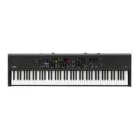
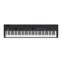
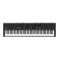
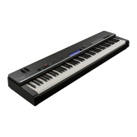
Overview of controls and indicators on the front of the unit.
Overview of connectors and ports on the rear of the unit.
Procedure for removing the top cover assembly.
Steps for removing various circuit boards and assemblies.
Procedure for removing the keyboard assembly from the unit.
Instructions for removing the left and right side covers.
Steps for removing the front rail assembly.
Detailed steps for disassembling the keyboard assembly.
Pin configuration and functions for the USB controller IC.
Pin configuration and functions for the DAC IC.
Pin configuration and functions for the CPU IC.
Pin configuration and functions for the CPU IC.
Pin configurations for LKS and E-PNS2a ICs.
Component layout and wiring diagram for the AJACK board.
Component layout and wiring diagram for the DJACK board.
Component layout and wiring diagram for the MVR board.
Component layout and wiring diagram for the PNL board.
Component layout and wiring diagram for the PNR board.
Component layout and wiring diagram for the SVR board.
Component layout and wiring diagram for the MK SUB board.
Component layout and wiring diagram for the GHD EBUS L board.
Component layout and wiring diagram for the GHD M board.
Component layout and wiring diagram for the GHD H board.
Required instruments, settings, and connections for testing.
Methods to access the product's test mode.
Steps for executing tests, interpreting results, and navigating.
Detailed list of tests, functions, and judgment criteria.
Using MIDI codes to select and execute test items.
Details on adjustable functions and their default values.
Settings specific to master mode operations.
Data formats for note and control change MIDI messages.
Data formats for mode and program change messages.
Data formats for system exclusive MIDI messages.
| Type | Stage Piano |
|---|---|
| Number of Keys | 88 |
| Polyphony | 64 |
| Voices | 14 |
| Effects | Reverb, Chorus |
| Key Action | Graded Hammer |
| Sound Engine | AWM (Advanced Wave Memory) |
| EQ | 3-band |
| Connectivity | MIDI In/Out, Sustain Pedal |