Do you have a question about the Yamaha R-V501 and is the answer not in the manual?
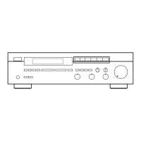
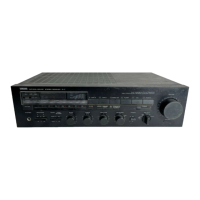
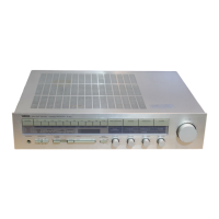
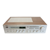
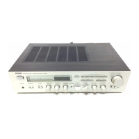
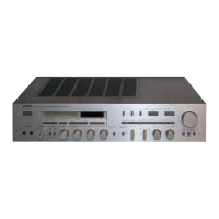
| Type | Stereo Receiver |
|---|---|
| Frequency Response | 20 Hz - 20 kHz |
| Input Sensitivity | 200 mV |
| Input Impedance | 47 kΩ |
| FM Tuner | Yes |
| AM Tuner | Yes |
| Bluetooth | No |
| Analog Audio Inputs | 4 |
| Analog Audio Outputs | 2 |
| Subwoofer Output | Yes |
| Headphone Output | Yes |
| Dimensions (W x H x D) | 17 x 5.25 x 14.5 in |
| Weight | 18 lbs |
| Digital Audio Inputs | 1 Optical, 1 Coaxial |
| Speaker Outputs | 2 pairs |
Manual provided for authorized retailers/service personnel with assumed basic service knowledge.
Failure to follow procedures may cause injury or product damage. Service by authorized retailer advised.
Static can destroy components; ground yourself to the unit's ground buss.
Specifications may change without notice due to continuous product improvement.
Components with special characteristics must be replaced with identical parts.
Verify insulation of conductive surfaces after service; measure leakage current.
Product contains lead and other chemicals; avoid contact and ingestion. Handle with care.
Detailed technical specifications for the audio output power, frequency response, and input sensitivity.
Technical specifications for video signal levels and frequency response.
Tuning range, sensitivity, selectivity, and distortion for FM reception.
Tuning range, sensitivity, selectivity, and distortion for AM reception.
Power supply, consumption, dimensions, weight, and accessories.
Procedures for initiating the self-check mode with or without factory preset.
How to exit the self-check mode and return to normal operation.
Information on factory preset values for Tuner, Surround, and Selector sections.
Details on the Main Bypass function (SELF 1) for audio output.
Explanation of the Display Check function (SELF 4) for FL display segments.
Operation of the Manual Test Tone function (SELF 5) for audio output.
Description of the Photograph Mode function (SELF 6) for display and cataloging.
Details on the Input Change Mode function (SELF 7) for input selection.
List of instruments needed for tuner adjustments.
Diagrams for setting up dummy antennas for FM and AM signals.
Diagram identifying key test points on the tuner PCB for adjustments.
Pre-adjustment steps including modulation and SG connection.
Wiring diagrams for discriminator balance, monaural distortion, and stereo adjustment tests.
Table detailing adjustment steps, test points, and expected ratings.
Steps for adjusting front end IFT, monaural, and stereo distortion.
Steps for adjusting sensitivity, separation, and signal meters.
Procedure to verify the automatic tuning function.
Diagram and steps for adjusting AM sensitivity and audio output.
Procedures for verifying AM sensitivity and auto-tuning.
Steps for adjusting RDS sensitivity and verifying program service name display.
Procedure to confirm and adjust idling current for front L/R amplifier sections.
Procedure to confirm and adjust idling current for the center amplifier section.
Pin configuration, I/O, and function for the M38114M8-104SP µ-COM IC.
Block diagram illustrating the internal structure and connections of IC301.
Detailed pinout and function descriptions for various ICs (P61-P37, P27-P00, etc.).
Table mapping port names to their I/O and specific functions.
Circuit diagrams and pinouts for NJM2068L-D and NJM2068D-D dual operational amplifiers.
Circuit diagram and control logic for the NJU7313 analog function switch.
Circuit diagram for the BA7612N 3-input video switch with 6dB amplifier.
Circuit diagram and control inputs for the TC4053BP triple 2-channel multiplexer.
Circuit diagram for the µPC1188H power amplifier.
Circuit diagram for the LB1641 motor driver.
Circuit diagram for the LA2785 Dolby Pro Logic surround matrix decoder.
Circuit diagram for the LV1010N Dolby Surround passive decoder.
Circuit diagram for the BU2090 serial in/parallel out driver.
Foil side view of the P.C.B. MAIN (1) and P.C.B. OPERATION (1) for RX-V390/R-V501.
Foil side view of the P.C.B. OPERATION (1) for RX-V390/R-V501.
Foil side view of the P.C.B. MAIN (3) for RX-V390/R-V501.
Table listing semiconductor component locations on the PCBs.
Foil side view of P.C.B. MAIN (1) for RX-V390RDS, showing component mounting.
Foil side view of P.C.B. MAIN (3) for RX-V390RDS, showing component mounting.
Foil side view of P.C.B. OPERATION (1) for RX-V390RDS.
Table listing semiconductor component locations on the PCBs.
Foil side view of P.C.B. TUNER for RX-V390/R-V501, showing adjustment points.
Foil side view of P.C.B. TUNER for RX-V390RDS, showing adjustment points.
Foil side view of P.C.B. INPUT (4) for RX-V390RDS.
Table listing semiconductor component locations on the Tuner and Input PCBs.
Foil side view of P.C.B. INPUT (3) and P.C.B. INPUT (1) boards.
Foil side view of P.C.B. OPERATION (2) and P.C.B. OPERATION (3) boards.
Table listing semiconductor component locations on the Input and Operation PCBs.
Foil side view of P.C.B. INPUT (5) and P.C.B. INPUT (6) boards.
Foil side view of P.C.B. MAIN (2) and P.C.B. MAIN (4) boards.
Foil side view of P.C.B. MAIN (2) for the A model.
Foil side view of P.C.B. MAIN (2) for the B model.
Oscilloscope waveforms for various test points, indicating signal characteristics.
Pin connection diagrams for various integrated circuits used in the unit.
Pinout diagrams for diodes and transistors.
Assignments for grid and anode connections on the display.
List of abbreviations used for electrical components in the parts list.
Detailed list of electrical components with part numbers, descriptions, and ratings.
List of components (VR, CB, C, D, F, IC, L, Q) found on the Tuner PCB.
List of components (SW, T, TP, VR, XL) on the Tuner PCB.
List of Main PCB assemblies and their associated components.
List of capacitors (C140-C166) and associated parts on the Main PCB.
List of transistors (Q101-Q124) and associated parts on the Main PCB.
List of resistors (R132-R193) and associated parts on the Main PCB.
List of connectors (CB301-CB304) and capacitors (C301-C304) on the Main PCB.
List of diodes, ICs, and transistors (D308-Q404) on Operation/Input PCBs.
List of switches (SW327-SW329) and PCB assemblies (VS966200-VS966600).
List of capacitors (C712-C791) and associated parts on the Input PCB.
List of diodes (D501-D712) and associated parts on the Input PCB.
List of resistors (R747-R813) and associated parts on the Input PCB.
List of relays, switches, and resonators (RY701-XL501) on the Input PCB.
List of mechanical parts related to the front panel and buttons.
List of PCB assemblies, chassis, and related hardware.
List of power cords, AC outlets, and associated parts.
List of knobs, speaker terminals, and related mechanical parts.