Do you have a question about the Yamaha RX-V377 Series and is the answer not in the manual?
Information on critical components requiring specific replacement parts.
Procedure for verifying insulation and measuring leakage current on 120V models.
Notice about chemicals in the product and safe handling of solder.
Information and recommendations for using lead-free solder during repairs.
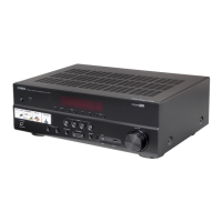
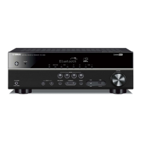
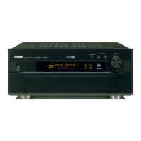
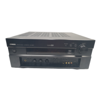
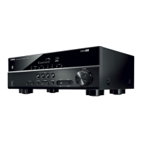
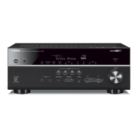
Front panel layout for various RX-V377 models.
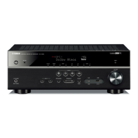
Front panel layout specific to the RX-V377 (T model).
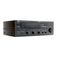
Front panel layout for various HTR-3067 models.
Front panel layout specific to the HTR-3067 (T model).
Rear panel connections for RX-V377 (U, C models).
Rear panel connections for RX-V377 (R, V, S models).
Rear panel connections for RX-V377 (T model).
Rear panel connections for RX-V377 (K model).
Rear panel connections for RX-V377 (A model).
Rear panel connections for RX-V377 (B, G, F models).
Rear panel connections for RX-V377 (L model).
Rear panel connections for RX-V377 (H model).
Rear panel connections for RX-V377 (J model).
Rear panel connections for HTR-3067 (U, C models).
Rear panel connections for HTR-3067 (R, S models).
Rear panel connections for HTR-3067 (T model).
Rear panel connections for HTR-3067 (K model).
Rear panel connections for HTR-3067 (A model).
Rear panel connections for HTR-3067 (G, F models).
Rear panel connections for HTR-3067 (L model).
Rear panel connections for HTR-3067 (H model).
Rear panel connections for HTR-3067 (J model).
Layout and function of the RAV521 remote control.
Layout and function for T model remote control sheet.
Detailed audio specifications including output power, dynamic power, and frequency response.
Detailed video specifications including signal types, levels, and frequency response.
Specifications for FM tuning range, sensitivity, and distortion.
Specifications for AM tuning range and antenna input.
General specifications including power supply, consumption, dimensions, and weight.
Available finishes for RX-V377 and HTR-3067 models.
List of included accessories with quantities.
Dimensional diagrams with measurements in millimeters and inches.
Settings for subwoofer, front, center, surround speakers, crossover, and phase.
Settings for speaker distance measurement in meters or feet.
Settings for adjusting speaker levels in dB.
Settings for equalizer selection (PEQ/GEQ) and GEQ edit.
Setting for enabling or disabling the test tone.
Settings for HDMI control, audio output, TV audio input, standby sync, and ARC.
Settings for sound DSP parameters like panorama, center width, dimension, and center image.
Settings for lipsync adjustment and scale.
Settings for automatic power standby time.
Procedure for renaming input sources and selecting preset names.
Diagram showing the internal components from the top view.
Diagram showing internal components from the front view.
Important safety precautions for servicing, including handling high voltages and capacitors.
Step-by-step instructions for removing the top cover.
Step-by-step instructions for removing the front panel unit.
Procedure for removing the DIGITAL P.C.B.
Procedure for removing the OPERATION (4) P.C.B.
Procedures for checking the DIGITAL P.C.B. using a checking jig.
Procedures for checking the MAIN (1) P.C.B. using ground leads.
How to check firmware version and checksum using the self-diagnostic function.
Procedure to initialize the backup IC after firmware update for proper setting storage.
List of tools required for firmware writing, including USB storage device and firmware file.
Steps to prepare for firmware update, including downloading and copying files to USB.
Steps for operating the firmware update process via USB.
Steps to start the firmware update process from USB.
Display messages indicating successful firmware writing and completion.
How to verify the firmware version after the update process.
Table listing error numbers, messages, and their causes.
Table listing main diagnostic menu items and their sub-menu items.
Diagnostic menu items related to network system functionality.
Diagnostic menu items for communication system and bus line checks.
Diagnostic menu items for checking HDMI information.
Diagnostic menu items related to video system checks.
Diagnostic menu items for radio system and tuner checks.
Diagnostic menu items for power supply and protection system monitoring.
Diagnostic menu items for troubleshooting and fault analysis information.
Diagnostic menu items for system and firmware version information.
Steps to start the self-diagnostic function by pressing specific keys.
Steps to enter self-diagnostic mode with protection functions disabled.
Steps to cancel the self-diagnostic function and preserve user memory.
Description of displays shown when the self-diagnostic function starts or is interrupted.
Information displayed when the protection function activates and shuts off power.
Diagnosis and checks for protection function activation due to excessive current.
Diagnosis and checks for protection function activation due to abnormal DC output.
Diagnosis and checks for protection function activation due to abnormal power supply voltage.
Diagnosis and checks for protection function activation due to excessive heatsink temperature.
How protection function history is stored and accessed.
How to navigate and operate the main and sub-menus for self-diagnosis.
Functions available during self-diagnostic mode, like power on/off and volume.
Default settings applied when the self-diagnostic function is initiated.
Menu for checking audio signal routes via DSP.
DSP audio signal output including head margin.
DSP subwoofer signal output with head margin, others without.
DSP audio output only to CENTER channel without head margin.
DSP audio output only to SURROUND L/R channels without head margin.
Diagnostic option for DSP full surround back, marked 'Not for service'.
DSP audio output to subwoofer channel without head margin.
Menu for checking audio signal routes in DIRECT mode.
Analog input audio signal output to FRONT L/R in DIRECT mode.
Diagnostic option for NET DIRECT, marked 'Not for service'.
Menu for checking audio signal input routes to HDMI IN/OUT jacks.
Displays the model name written to the HDMI module.
Menu for checking speaker output status.
Mutes audio signals for all channels.
Menu for checking MIC input signal route via YPAO.
Checks audio signal input to YPAO MIC jack output.
Diagnostic option marked 'Not for service'.
Diagnostic option for DIR PLL, marked 'Not for service'.
Menu for testing noise generator output to channels.
Outputs test noise to all channels.
Diagnostic option marked 'Not for service'.
Menu for checking the operation of the FL display.
Checks for shorts between adjacent segments in a lattice pattern.
Checks for shorts between adjacent segments in a lattice pattern.
Menu to check audio signal route from USB storage device.
Reproduces the first music file stored on the USB device.
Checks SPI communication between microprocessor and USB controller.
Diagnostic option marked 'Not for service'.
Checks the Apple authentication IC device ID.
Diagnostic option marked 'Not for service'.
Checks communication and bus line connections on the DIGITAL P.C.B.
Displays the total detection result of sub-menus C1-2 to C1-8.
Checks reading/writing of microprocessor and OSD FLASH ROM.
Checks reading/writing of OSD FLASH ROM and HDMI IC.
Diagnostic option for VIDEO I/F, marked 'Not for service'.
Checks communication and bus line connection between microprocessor and DIR.
Checks communication and bus line connection between microprocessor and DSP.
Checks reading of EEPROM.
Checks AM/FM TUNER I2C bus line connection.
Menu to display information about HDMI.
Displays the model name written to the HDMI module.
Diagnostic option for HDMI product ID, marked 'Not for service'.
Diagnostic option marked 'Not for service'.
Menu to check the analog video signal route.
Shows how the video signal is converted and output.
Checks if the video signal is muted.
Menu to check the digital video signal route.
Checks if video/audio signals input to HDMI IN jack are output to HDMI OUT jack.
Checks if the 'OSD CHECK' screen is output to HDMI OUT jack.
Diagnostic option marked 'Not for service'.
Displays A/D conversion values of microprocessor for panel keys and protection functions.
Detects power amplifier DC (DC voltage) output.
Detects power supply voltage (PS) protection.
Detects heatsink temperature by voltage measurement.
Detects output level of speaker output.
Detects power limiter control.
Diagnostic option marked 'Not for service'.
Detects panel keys and checks their A/D conversion values.
Displays the history of protection function operations.
Stores setting information for protection function operations.
Diagnostic item related to power port, marked 'Not for service'.
Displays the last selected input source in hexadecimal notation.
Displays the last selected volume level.
Displays the operating time of the unit.
Displays the operation frequency of the power relay.
Displays the operation frequency of the POWER AMP B relay.
Displays the maximum value of the speaker output level.
Diagnostic option marked 'Not for service'.
Allows updating the unit's firmware.
Displays the model name and destination.
Menu to reserve or inhibit backup IC initialization.
Displays firmware version and checksum values.
Displays the main firmware version.
Displays firmware version of the microprocessor.
Displays firmware version of the DSP.
Displays firmware version of OSD data.
Switches between PCB and MODEL write modes for backup IC.
Selects the desired model name to write to the backup IC.
Selects the desired destination to write to the backup IC.
Diagnostic option for USB controller version, marked 'Not for service'.
Diagnostic option for USB controller checksum, marked 'Not for service'.
Selects and writes the desired model name to the backup IC.
Selects and writes the desired destination to the backup IC.
Displays the model name and destination.
Diagnostic option marked 'Not for service'.
Procedure to confirm voltage across power amplifier terminals after power on.
Pin assignment and function details for IC241 on the DIGITAL P.C.B.
Detailed pin functions and their corresponding I/O and purpose.
Detailed pin functions and their corresponding I/O and purpose.
Detailed pin functions and their corresponding I/O and purpose.
Detailed pin functions and their corresponding I/O and purpose.
Pin assignment and function details for the microprocessor IC221.
Detailed pin functions for various ports and their associated functions.
Detailed pin functions for various ports and their associated functions.
Detailed pin functions for various ports and their associated functions.
Block diagram for the main audio signal flow.
Block diagram for operation and control signals.
Block diagram for digital signal processing and connections.
Component layout diagram for the DIGITAL P.C.B. (Side A).
Component layout diagram for the DIGITAL P.C.B. (Side B).
Component layout diagrams for OPERATION P.C.B.s (Sides A).
Component layout for the OPERATION (2) P.C.B. (Side B).
Component layout for the OPERATION (3) P.C.B. (Side B).
Component layout for the MAIN (1) P.C.B. (Side A).
Component layout for the OPERATION (2) P.C.B. (Side A).
Component layout for the OPERATION (3) P.C.B. (Side A).
Component layout for the OPERATION (2) P.C.B. (Side B).
Component layout for the OPERATION (3) P.C.B. (Side B).
Component layout for the OPERATION (4) P.C.B. (Side A).
Component layout for the OPERATION (5) P.C.B. (Side A).
Component layout for the OPERATION (6) P.C.B. (Side A).
Component layout for the OPERATION (7) P.C.B. (Side A).
Component layout for the OPERATION (4) P.C.B. (Side B).
Component layout for the OPERATION (5) P.C.B. (Side B).
Component layout for the OPERATION (6) P.C.B. (Side B).
Component layout for the OPERATION (7) P.C.B. (Side B).
Component layout for the MAIN (1) P.C.B. (Side A).
Component layout for the OPERATION (4) P.C.B. (Side A).
Component layout for the OPERATION (5) P.C.B. (Side A).
Component layout for the MAIN (1) P.C.B. (Side B).
Component layout for the MAIN (2) P.C.B. (Side A).
Component layout for the MAIN (3) P.C.B. (Side A).
Component layout for the MAIN (4) P.C.B. (Side A).
Component layout for the MAIN (5) P.C.B. (Side A).
Component layout for the MAIN (2) P.C.B. (Side B).
Component layout for the MAIN (3) P.C.B. (Side B).
Component layout for the MAIN (4) P.C.B. (Side B).
Component layout for the MAIN (5) P.C.B. (Side B).
Pin connection diagrams for various ICs used in the unit.
Pin connection diagrams for various diodes.
Pin connection diagrams for various transistors.
Schematic diagram for the DIGITAL section, part 1 of 5.
Schematic diagram for the DIGITAL section, part 2 of 5.
Schematic diagram for the DIGITAL section, part 3 of 5.
Schematic diagram for the DIGITAL section, part 4 of 5.
Schematic diagram for the DIGITAL section, part 5 of 5.
Schematic diagrams for OPERATION sections 1 through 7.
Schematic diagram for OPERATION (2) P.C.B. (Side A).
Schematic diagram for OPERATION (2) P.C.B. (Side B).
Schematic diagram for OPERATION (3) P.C.B. (Side A).
Schematic diagram for OPERATION (3) P.C.B. (Side B).
Schematic diagram for the MAIN (1) section.
Schematic diagram for MAIN (1) section, showing signal flow.
Schematic diagram for MAIN (2) section.
Schematic diagram for MAIN (3) section.
Schematic diagram for MAIN (4) section.
Schematic diagram for MAIN (5) section.
Schematic diagram for MAIN (2) section.
Schematic diagram for MAIN (3) section.
Schematic diagram for MAIN (4) section.
Schematic diagram for MAIN (5) section.
Warning regarding special characteristic components and replacement parts.
List of abbreviations used in the replacement parts list.
Replacement parts list for DIGITAL P.C.B. components.
Replacement parts list for DIGITAL P.C.B. components.
Replacement parts list for DIGITAL P.C.B. components.
Replacement parts list for OPERATION P.C.B. components.
Replacement parts list for MAIN P.C.B. components.
Replacement parts list for OPERATION P.C.B. components.
Replacement parts list for MAIN P.C.B. components.
Replacement parts list for MAIN P.C.B. components.
Replacement parts list for MAIN P.C.B. components.
Replacement parts list for MAIN P.C.B. components.
List of included accessories with part numbers and descriptions.
Schematic diagram of the RAV521 remote control.
Layout of the RAV521 remote control panel buttons.
Remote control sheet specific to the T model.
Table mapping key codes to functions, ID settings, and remote sheet labels.
How to change the remote control ID to match the receiver's ID.
How to adjust FM/AM tuning frequency based on listening environment.
How to change the HDMI output video signal type (NTSC/PAL).
Options to restore all default settings or cancel initialization.
Information on updating firmware via USB for new features or fixes.
Step-by-step instructions for updating the unit's firmware.
How to change the remote control ID to match the receiver's ID.
How to switch the HDMI output video signal type (NTSC/PAL).
Options to restore all default settings or cancel initialization.
Information on updating firmware via USB for new features or fixes.
Step-by-step instructions for updating the unit's firmware.
Crucial warnings about using only official firmware and following instructions carefully.
Steps to prepare the USB drive with the firmware file.
Instruction to power off the receiver before starting the update.
Instructions on where to insert the USB thumb drive.
Steps to access the ADVANCED SETUP mode for firmware update.
How to select the firmware update option from the ADVANCED SETUP menu.
Steps to initiate the firmware update process using the INFO key.
Warnings against interrupting power during the update process.
How to verify the firmware version after the update is complete.
Congratulatory message upon successful firmware update.
Troubleshooting steps for error messages during firmware update.
Troubleshooting steps when firmware update fails to start or after update.
Crucial warnings about using only official firmware and following instructions carefully.
Steps to prepare USB, copy firmware, and enter ADVANCED SETUP mode.
How to select the FIRM UPDATE USB option from the menu.
Steps to initiate the firmware update process using the INFO key.
How to check the firmware version after the update is completed.
Troubleshooting steps for error messages during firmware update.
Troubleshooting steps when firmware update fails to start or after update.
Troubleshooting steps for remote control malfunctions, possibly due to ADVANCED SETUP settings.
| Channels | 5.1 |
|---|---|
| HDMI Inputs | 4 |
| HDMI Outputs | 1 |
| YPAO Sound Optimization | Yes |
| Response Bandwidth | 10Hz-100kHz |
| Signal-To-Noise Ratio | 100 dB |
| Input Sensitivity | 200 mV |
| Audio D/A Converter | 192 kHz/24-bit |
| Output Impedance / Channel | 6 ohms |
| Frequency Response | 10Hz-100kHz |
| Tuner Type | Digital |
| Tuner Bands | AM/FM |
| Bluetooth | No |
| Power Output | 100W per channel (1kHz, 1ch driven, 6 ohms, 0.9% THD) |
| Dolby Technologies | Dolby Digital Plus |
| DTS Technologies | DTS-HD Master Audio |
| Amplifier Output Details | 100W per channel (1kHz, 1ch driven, 6 ohms, 0.9% THD) |
| Input Impedance | 47k ohms |
| Output Power / Channel | 100W (6 ohms, 1 kHz, 0.9% THD, 1 channel driven) |
| USB Input | Yes (iPod / iPhone / USB memory devices) |