Do you have a question about the Yamaha RX-V870 and is the answer not in the manual?
Advises on safety procedures and recommends authorized service personnel for repairs.
Warns about static discharge destroying components and provides grounding advice.
Instructs to turn the unit OFF during disassembly and parts replacement.
Information for service personnel regarding critical components and procedures.
Illustrations of front and rear panel controls and connectivity.
Detailed technical specifications for audio, video, FM, and AM sections.
Information on replacing critical components with identical specifications.
Procedure for verifying leakage current after service for safety.
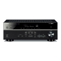
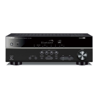
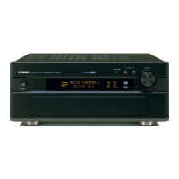
Illustration of the RX-V1070 front panel controls.
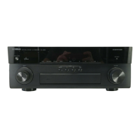
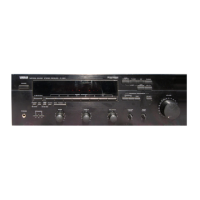
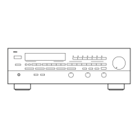
Illustration of the RX-V870 front panel controls.
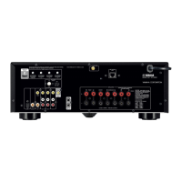
Diagram of the rear panel connections for the U.S.A. model.
Diagram of the rear panel connections for the Canadian model.
Diagram of the rear panel connections for the Australian model.
Diagram of the rear panel connections for the General model.
Details on output power, input sensitivity, damping factor, and distortion.
Details on video signal types, levels, and frequency response.
Specifications for tuning range, sensitivity, distortion, and separation.
Specifications for tuning range, sensitivity, selectivity, and distortion.
Details on power supply, consumption, AC outlets, and accessories.
Physical dimensions (W x H x D) and weight of the receiver.
Block diagram showing the video signal processing path for RX-V1070.
Block diagram illustrating the processing of audio signals from various inputs.
Exploded view showing the internal layout of major components and PCBs.
Step-by-step guide for disassembling the unit to access internal components.
Instructions for removing the power transistor using specific tools.
Details on protection function activation, circuit elements, and microcomputer roles.
Step-by-step guide for adjusting idling current, including test points and ratings.
Diagrams and labels for test points and adjustment points on the Tuner PCB.
Settings required before performing tuner adjustments, including modulation and switch positions.
Procedure and connection diagram for adjusting discriminator balance.
Procedure and connection diagram for adjusting monaural distortion.
Procedure and connection diagram for adjusting stereo distortion and separation.
Procedure to minimize stereo distortion and ensure stereo indicator lights.
Procedure to verify monaural distortion level.
Procedure for verifying FM sensitivity across different frequencies and input voltages.
Procedure to minimize signal leakage between channels for stereo separation.
Procedure for adjusting AM section sensitivity, signal meter, and auto tuning.
Procedure to maximize audio output by adjusting AM sensitivity.
Procedure to verify AM sensitivity and distortion levels at different frequencies.
Procedure to verify signal meter indication for AM reception.
Instructions on how to initiate and terminate the self-diagnosis mode.
Tests all segments of the LCD display by turning them on.
Checks LED lighting sequence and LCD inhibit function.
Tests DSP through A path for FL/FR, RL/RR, and CENTER output signals.
Tests DSP through B path for MAIN L/R, CENTER, and RL/RR output signals.
Tests RAM through path for MAIN L/R, CENTER, and RL/RR output signals.
Disables auto input balance and tests Pro Logic mode.
Outputs manual test tones (L, C, R, S) for verification.
Detailed pinout, function, and block diagram for the 8-bit microcomputer IC720.
Detailed table of pin functions and states (Power On, Power Off, Back Up) for IC720.
Pinout and function details for the Digital Dolby Pro Logic Decoder IC503.
Detailed table of pin names, I/O types, and functions for IC503.
Illustrations of LCD display patterns and a table mapping display segments to functions.
Foil side layout diagram for the RX-V1070/V870 DSP Printed Circuit Board (1).
Foil side layout diagram for the RX-V1070/V870 DSP Printed Circuit Board (2).
Foil side layout diagram for the RX-V1070/V870 DSP Printed Circuit Board (3).
Foil side layout diagram for the RX-V1070/V870 Operation Printed Circuit Board (1).
Detailed foil side layout for the RX-V1070/V870 DSP Printed Circuit Board (3).
Foil side layout diagram for the RX-V1070 Operation Printed Circuit Board (2).
Foil side layout diagram for the RX-V1070 Input Printed Circuit Board (2).
Foil side layout diagram for the RX-V870 Input Printed Circuit Board (2).
Foil side layout diagram for the RX-V1070/V870 Input Printed Circuit Board (3).
Foil side layout diagram for the RX-V1070/V870 Input Printed Circuit Board (4).
Foil side layout diagram for the RX-V1070/V870 Input Printed Circuit Board (5).
Foil side layout diagram for the RX-V1070 Main Printed Circuit Board (2).
Foil side layout diagram for the RX-V870 Main Printed Circuit Board (2).
Foil side layout diagram for the RX-V1070 Main Printed Circuit Board (1).
Foil side layout diagram for the RX-V1070 Main Printed Circuit Board (8).
Foil side layout diagram for the RX-V870 Main Printed Circuit Board (1).
Foil side layout diagram for the RX-V870 Main Printed Circuit Board (8).
Foil side layout diagram for the RX-V1070 Main Printed Circuit Board (4).
Foil side layout diagram for the RX-V1070 Main Printed Circuit Board (3).
Foil side layout diagram for the RX-V1070 Main Printed Circuit Board (5).
Foil side layout diagram for the RX-V1070 Main Printed Circuit Board (6).
Foil side layout diagram for the RX-V870 Main Printed Circuit Board (4).
Foil side layout diagram for the RX-V870 Main Printed Circuit Board (5).
Foil side layout diagram for the RX-V870 Main Printed Circuit Board (3).
Foil side layout diagram for the RX-V870 Main Printed Circuit Board (6).
Foil side layout diagram for the RX-V1070 Main Printed Circuit Board (9).
Foil side layout diagram for the RX-V1070 Main Printed Circuit Board (3).
Foil side layout diagram for the RX-V1070 Main Printed Circuit Board (6).
Foil side layout diagram for the RX-V870 Main Printed Circuit Board (9).
Oscilloscope waveform for IC503, Pin 51, showing voltage and time scales.
Oscilloscope waveform for IC501, Pin 15, showing voltage and time scales.
Oscilloscope waveform for IC501, Pins 23-26, showing voltage and time scales.
Oscilloscope waveform for IC501, Pin 27, showing voltage and time scales.
Oscilloscope waveform for IC519, Pin 50, showing voltage and time scales.
Oscilloscope waveform for IC519, Pin 55, showing voltage and time scales.
Oscilloscope waveform for IC519, Pin 64, showing voltage and time scales.
Oscilloscope waveforms for IC720 Pin 8 and D710 Anode.
Detailed circuit schematic for the tuner and operation control sections.
Circuit details for tuner components including ICs, transistors, and coils.
Schematic showing tuner signal paths and preset station control connections.
Detailed circuit schematic for the Digital Sound Field Processor (DSP) section.
Schematic illustrating the signal flow within the DSP section.
Detailed circuit schematic for all audio and video input sections.
Pin connection diagram for µPC4570HA Dual Op-amp ICs.
Pin connection diagram for µPC4570C Dual Op-amp IC.
Pin connection diagram for TC4051 Single 8-Channel Multiplexers.
Schematic for tone control, electric controlled volume, and motor drive circuits.
Pin connection diagram for TC4069UBP/µPD4069C Hex Inverter IC.
Pin connection diagram for BA6229 Motor Driver IC.
Pin connection diagram for LC7535 Electric Controlled Volume ICs.
Schematic for system control, analog function switch, and various IC pinouts.
Pinout for TC4051 multiplexer/demultiplexer ICs.
Pinout for µPD4066BC Quad Bilateral Switch ICs.
Pinout for µPD4052BC/TC4052BP Analog Multiplexer IC.
Schematic detailing input/output connections and internal processing within the DSP section.
Schematics for key ICs within the DSP section, including op-amps and multiplexers.
Schematic diagram for the display drive circuitry, including IC519.
Pinout and functional description for the high-speed pseudo static RAM IC501.
Pinout and function details for the LC7582 LCD Driver IC.
Pinout for TC4053BP/µPD4053BC Triple Analog Multiplexer IC.
Detailed circuit schematic for the main section of the RX-V1070 receiver.
Schematic for RX-V1070 front, center power amplifiers and protection circuit.
Circuit diagram for the STK4151V power amplifier IC.
Schematic for the RX-V1070 rear power amplifier section.
Detailed circuit schematic for the main section of the RX-V870 receiver.
Schematic for RX-V870 front, center power amplifiers and protection circuit.
Circuit diagram for the STK4141V power amplifier IC.
List of components for the RX-V1070 Main and Input Printed Circuit Boards.
Component list for the RX-V1070 Main Printed Circuit Board.
List of resistors for the RX-V1070 Main Printed Circuit Board.
List of components for the RX-V870 Main Printed Circuit Board.
List of components for the RX-V1070 Input Printed Circuit Board.
Component details for the RX-V1070 Input Printed Circuit Board.
List of transistors for the RX-V870 Main Printed Circuit Board.
List of resistors for the RX-V870 Main Printed Circuit Board.
List of capacitors for RX-V1070 Main and Input PCBs.
Component details for capacitors on the RX-V1070 Input Printed Circuit Board.
List of components for RX-V870 Input and DSP Printed Circuit Boards.
Component details for capacitors on the RX-V870 DSP Printed Circuit Board.
List of resistors for the RX-V870 DSP Printed Circuit Board.
List of components for RX-V870 DSP and Tuner Printed Circuit Boards.
Component list for RX-V870 Tuner and Operation Printed Circuit Boards.
List of capacitors for the RX-V870 Main Printed Circuit Board.
List of transistors for the RX-V870 Main Printed Circuit Board.
List of resistors for the RX-V870 DSP Printed Circuit Board.
List of components for RX-V870 Main and Input Printed Circuit Boards.
Component details for the RX-V870 Input Printed Circuit Board.
List of components for RX-V870 Input and DSP Printed Circuit Boards.
Component details for capacitors on the RX-V870 DSP Printed Circuit Board.
List of resistors for the RX-V870 DSP Printed Circuit Board.
List of components for RX-V870 DSP and Tuner Printed Circuit Boards.
Component list for RX-V870 Tuner and Operation Printed Circuit Boards.
Exploded view diagram of the RX-V1070 panel unit components.
List of mechanical parts for the RX-V1070, including reference numbers and descriptions.
List of mechanical parts for the RX-V870, including reference numbers and descriptions.
Continued list of mechanical parts for the RX-V1070.
List of accessories included with the RX-V1070 unit.
Detailed exploded view of the RX-V1070 panel unit components.
Schematic diagram of the remote control transmitter's circuitry.
Table mapping remote control button codes to their functions.
List of carbon resistors with part numbers for 1/4W and 1/6W types.
| Brand | Yamaha |
|---|---|
| Model | RX-V870 |
| Category | Stereo Receiver |
| Language | English |