Do you have a question about the Yamaha RX-Z7 and is the answer not in the manual?
Information on critical components that must be replaced with identical specifications.
Verifying insulation of exposed surfaces from supply circuits post-service.
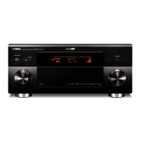
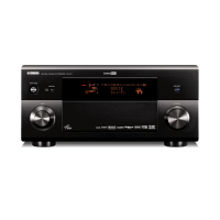
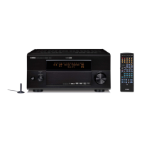
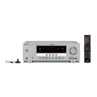
Illustration and labeling of the front panel for RX-Z7 (U, C models).
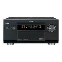
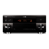
Illustration and labeling of the front panel for RX-Z7 (A model).
Illustration and labeling of the rear panel for RX-Z7 (U model).
Layout and labels for the RAV389 remote control used with U, C models.
Layout and labels for the RAV391 remote control used with various models.
Technical specs for audio section: output power, frequency response, distortion, S/N ratio.
Technical specs for video section: signal types, conversion, levels, response.
Diagram showing internal components visible from the top.
Step-by-step procedure for removing the top cover.
Step-by-step procedure for removing the sub chassis unit.
Step-by-step procedure for removing the amplifier unit.
List of tools required for firmware updates.
How to confirm firmware version and checksum using the self-diagnostic function.
Main menu items related to audio settings and system configuration.
Main menu items related to the display system and FL check.
Main menu items for confirming zone function and input sources.
How to enter the self-diagnostic mode.
Displaying A/D conversion values for microprocessor, panel keys, and protection functions.
Displaying firmware version and checksum for various components.
Confirming the idling current of the amplifier unit after power on and after 60 minutes.
Diagrams showing pin connections for various integrated circuits.
Overall block diagram of the audio signal path.
Overall block diagram of the video signal path.
Top view layout of the DSP P.C.B. with component locations.
Top view layout of the FUNCTION (1) P.C.B. with component locations.
Top view layout of the MAIN (1) P.C.B. with component locations.
Top view layout of the POWER (1) P.C.B. with component locations.
Top view layout of the A-VIDEO P.C.B. with component locations.
Top view layout of the D-VIDEO (1) P.C.B. with component locations.
Top view layout of the FL (1) P.C.B. with component locations.
Top view layout of the CONNECT (1) P.C.B. with component locations.
Top view layout of the DCCNVT (1) P.C.B. with component locations.
Schematic diagram of the DSP section, part 1 of 3.
Schematic diagram of the FUNCTION section, part 1 of 4.
Lists various electrical components with their part numbers and specifications.
Replacement parts list for the DSP P.C.B.
Replacement parts list for the FUNCTION P.C.B.
Replacement parts list for the D-VIDEO P.C.B.
Replacement parts list for the POWER P.C.B.
Replacement parts list for the MAIN P.C.B.
Setting the color encoding format for television.
Activating or deactivating the monitor check function.
Selecting the display language for GUI, OSD, and messages.
Updating the unit's firmware using USB memory or network.
| Channels | 7.1 |
|---|---|
| Amplifier Type | Discrete |
| Signal-to-Noise Ratio | 100 dB |
| HDMI Inputs | 6 |
| HDMI Outputs | 2 |
| Audio Decoding | Dolby TrueHD, DTS-HD Master Audio |
| Power Output | 140W (8 ohms, 20 Hz - 20 kHz, 0.04% THD, 2ch driven) |
| Frequency Response | 10 Hz - 100 kHz |
| Total Harmonic Distortion (THD) | 0.04% |
| Input Sensitivity | 200 mV |
| Dimensions (W x H x D) | 435 x 171 x 435 mm |
| Network Features | Ethernet |
| USB Port | Yes |
| Video Upscaling | Yes (up to 1080p) |