module is installed in COMM and parameter “bAud” is set to 1, then on-off signal can be inputted, and SV1
and SV2 can be switched by connecting a switch between terminals 3 and 4.
Wiring graph of D2 dimension instruments (48*48mm)
P.S.:0-5 1-5 is not available ,transfer to 0-500mV or 100-500mV
input. 4-20mA input need add resistant 25ohm so that change to
100-500mV, then connect terminal 9 and 8. Terminal 3.4.5 is
for communcation S,S4. L5 is installed then need change bAud
as 0.
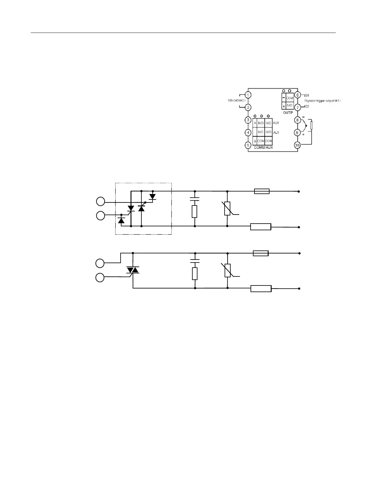
Wiring graph of thyristor trigger output is as below (suitable for module K1, K3, K5 and K6):
Capacitor Resistor
Absorber Circuit
Capacitor Resistor
Absorber Circuit
Note 1: According to the voltage and current of load, choose suitable varistor to protect the thyristor.
Capacitor resistor absorber is needed for inductance load or phase-shift trigger output.
Note 2: SCR power module is recommended. A power module includes two SCRs, is similar to the above
dashed square.
Note 3: K1/K3/K5 is burnt free, easy and reliable.
Note 4: Phase-shift trigger module K5 only supports 200~380VAC power, power frequency must be 50Hz.
 Loading...