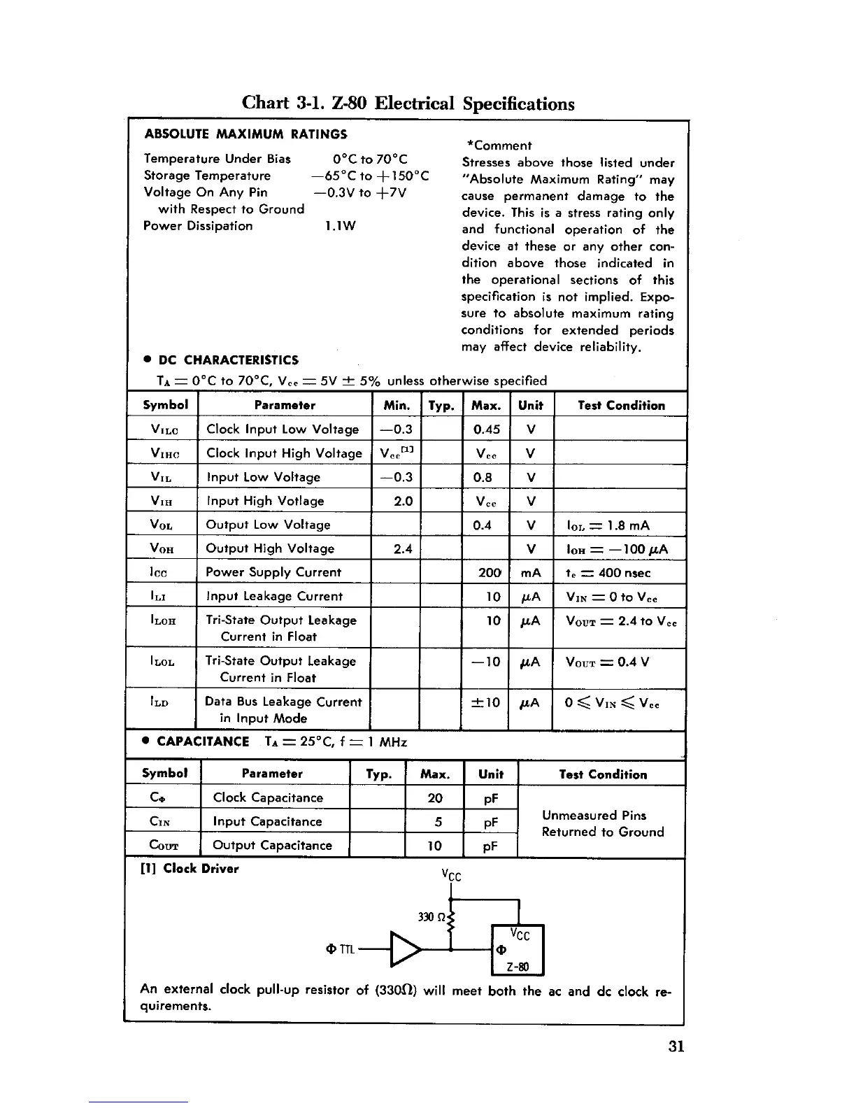
Chart
3-1. Z-80 Electrical Specifications
ABSOLUTE MAXIMUM RATINGS
*Comment
Temperature Under Bias 0
°C to 70°
C Stresses
above
those listed under
Storage
Temperature -65°C to x-150°C "Absolute Maximum
Rating" may
Voltage On Any Pin -0.3V to +7V cause permanent
damage to the
with Respect
to Ground device. This is a stress
rating only
Power Dissipation
1.1W and functional
operation of the
device at these
or any
other con-
dition above
those indicated in
the operational
sections of this
specification
is not implied. Expo-
sure
to absolute
maximum rating
conditions for extended
periods
may affect device reliability.
• DC CHARACTERISTICS
TA = 0°C to 70°C, V_ - 5V ± 5% unless
otherwise
specified
Symbol
Parameter
Min.
Typ
.
Max.
Unit
Test Condition
VILe
Clock Input Low Voltage
-0.3
0.45
V
Vine
Clock Input High Voltage
V°„m
V°°
V
VIL
Input Low Voltage
-0.3
0.8 V
Viii
Input High Votlage
2.0
V°°
V
VOL
Output Low Voltage
0.4 V
IOL = 1.8 mA
Vox
Output High Voltage
2.4
V
Ion = -100 µA
Ice
Power Supply Current
200
mA
t„ = 400 nsec
I
Lr
Input Leakage Current
10
µA
VIN = 0 to V°°
ILOH
Tri-State Output
Leakage
10
11A
VOUT = 2.4 to V°°
Current
in Float
ILOL
Tri-State
Output Leakage
-10
µA
VouT = 0.4 V
Current in Float
I
Ln
Data Bus Leakage Current
±10
µA
0 < VIN < V°°
in Input Mode
• CAPACITANCE
TA = 25°C, f - 1 MHz
Symbol
Parameter
Typ.
Max
.
Unit
Test Condition
Co
Clock
Capacitance
20
pF
CIN
Input Capacitance
5
pF
Unmeasured Pins
R
d
G
d
eturne
to
roun
COOT
Output
Capacitance
10
pF
[1] Clock Driver yCC
330 4
yCC
4 TTL m
Z-80
An external clock pull
-
up resistor
of (33012) will meet both
the ac and dc clock re-
quirements.
31
 Loading...