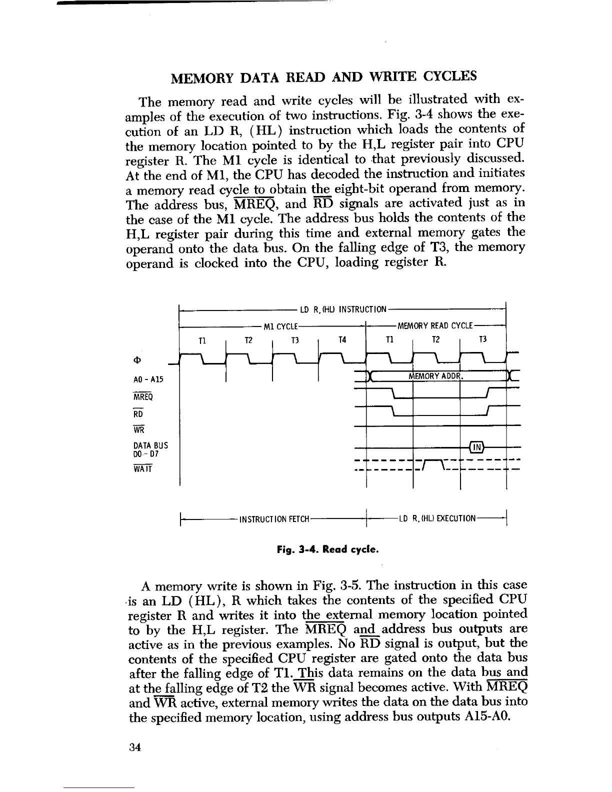
MEMORY DATA READ AND WRITE CYCLES
The memory read and write cycles will be illustrated with ex-
amples of the execution of two instructions. Fig. 3-4 shows the exe-
cution of an LD R, (HL) instruction which loads the contents of
the memory location pointed to by the H,L register pair into CPU
register R. The M1 cycle is identical to that previously discussed.
At the end of M1, the CPU has decoded the instruction and initiates
a memory read cycle to obtain the eight-bit operand from memory.
The address bus, MREQ, and RD signals are activated just as in
the case of the M1 cycle. The address bus holds the contents of the
H,L register pair during this time and external memory gates the
operand onto the data bus. On the falling edge of T3, the memory
operand is clocked into the CPU, loading register R.
Ti
- M1 CYCLE
T2 , T3
LD R,(HU INSTRUCTION
AO-A15
MREQ
RD
WR
DATA BUS
DO-D7
WAIT
LD R.(HL) EXECUTION--{
Fig. 3-4.
Read cycle.
A memory write is shown in Fig. 3-5. The instruction in this case
is an LD (HL), R which takes the contents of the specified CPU
register R and writes it into the external memory location pointed
to by the H,L register. The MREQ and address bus outputs are
active as in the previous examples. No RD signal is output, but the
contents of the specified CPU register are gated onto the data bus
after the falling edge of T1. This data remains on the data bus and
at the falling edge of T2 the WR signal becomes active. With MREQ
and WR active, external memory writes the data on the data bus into
the specified memory location, using address bus outputs A15-AO.
T4
-MEMORY READ CYCLE-
T1 T2 i T3
MEMORY ADDR.
INSTRUCTION FETCH
34
 Loading...