1. Product Specification (continued)
1.3.1.3 Audio Jack (option)
This jack shall connect the audio input from host
computer.
1.3.2 Video Input Signals
1.3.2.1 Video Signal Amplitudes
The three video inputs consist of Red ,Green , and Blue
signals, each with its own coaxial cable terminated at the
monitor. These video signals are analog levels, where 0
V corresponds to black , and 700 mV is the maximum
signal amplitude for the respective color, when each
signal is terminated by a nominal 75.0 ohms .For a given
monitor luminance levels are measured using this
defined video amplitud driving a monitor meeting the
termination requirements .The signal amplitude is not to
be readjusted to compensate for variations in termination
impendance.
1.3.2.2 Video Signal Termination Impedance
This analog video signal termination shall be 75 1%
which shall be resistive with a negligible reactive
component
1.3.2.3 Synchronization ( Sync ) Signals
The Horizontal Sync (HS) TTL signal is used to initiate
the display of a horizontal line. HS may be either active
high or active low, depending upon the timing .The
Vertical Sync (VS) TTL signal is used to initiate the
display of a new frame .VS may be either active high or
active low, depending on the timing
1.3.2.4 Sync Signal Levels
The monitor must accept sync signals from both 3.3 and
5 volt TTL logic families.The inputs shall sense a logic 0
when the input is 0.8 volt or less and shall sense a logic
1 when the input is 2.0 volts or greater. In addition to
these level requirements, there shall also be a minimum
of 0.3 volt hysteresis provided for noise immunity
(typically by using a Schmitt Trigger input ).That is , the
input level at which the monitor actually detects a logic 0
shall be at least 0.3 volt lower than the level at which it
actually detects a logic 1.If the monitor sync processing
circuits are designed around the 3.3 volt logic family
,then the sync inputs must be 5 volt tolerant .
TTL input loading shall be equivalent to one TTL input
load. When logic 0 is asserted by a sync input , the
maximum current source from any single monitor sync
input to the driver is 1.6 mA .When logic 1 is asserted ,
the maximum current source from the driver to any
single monitor sync input is 400 uA .
Ω+/-
.
1.3.2.5 Sync Signal Loading
DSUB
P in S ign a l P in S ig n a l P in S ig n al
1
Red-V ideo
6
Red-GND
11
NC
2
G reen-V ideo
7
Green-GND
12
DDC-SDA
3
Blue-Video
8
Blue-GND
13
H-SYNC
4
NC
9
+5V
14
V-SYNC
5
DDC-GND
10
Sync-G ND
15
DDC-SCL
Connector Pin A ssignm ent
D-SUB Pin Description
Pin N am e D escription
1 Red-Video Red video signal input.
2 Green-Video Green video signal input.
3 B lue - V id e o B lue v id e o s igna l inp u t .
4GND Ground
5 D D C - G N D D D C gro und fo r the V E S A D D C 2 B i func tio n.
6 R e d - G N D A na lo g s igna l gro und fo r the R e d vid e o .
7 G r ee n - G N D A na lo g signal gr o und fo r the G re e n vid e o .
8 B lue - G N D A na lo g s igna l gro und fo r the B lue vid e o .
9 + 5V + 5V inp ut fro m host system fo r the V ES A DD C 2 Bi functio n.
1 0 S y nc- G N D S igna l gro un d
11 GN D Ground
1 2 D D C _ S D A S D A signa l input fo r the V E S A D D C B 2 i func tio n.
13 H -S Y N C H orizonta l signal input from the host system .
14 V -S Y N C V ertica l signal inp ut from the host system.
1 5 D D C - S C L S C L s igna l inp ut fo r the V E S A D D C 2 B i functio n.
Connector Pin Description
DVI-I / DVI-D (If using DVI-D cable, C1, C2, C3, C4, C5 is NC)
Pin Signa l Pin Signa l Pin Signa l
1
RX2-
11
GND
21
NC
2
RX2+
12
NC
22
GND
3
GND
13
NC
23
RXC+
4
NC
14
5V
24
RXC-
5
NC
15
GND
C1
Analog Red (NC)
6
SCL
16
HP
C2
Analog Green (NC)
7
SCA
17
RX0-
C3
Analog Blue (NC)
8
Analog V-Sync (NC)
18
RX0+
C4
Analog H-Sync (NC)
9
RX1-
19
GND
C5
GND
10
RX1+
20
NC
DV I-I / DVI-D Con n ector P in Descr iption
P in Name D escrip tion P in Name Descrip tion
1 R X 2- T M D S li n k #0 ch an n el #2 di ff eren ti al pair 16 H P H ot pl u g g in g
2 RX2+ TMDS link #0 channel #2 differential pair 17 RX0- TMDS link #0 channel #0 differential pair
3 GND GND for no link share 18 RX0+ TMDS link #0 channel #0 differential pair
4 NC NC 19 GND GND for no link share
5NC NC 20NC NC
6 SCL Clock li ne for D D C in terface 21 NC NC
7 SDA Data line for DDC interface 22 GND Clock s hield
8
Analog
V- Sync
V-sync for analog interface 23 RXC+ TMDS clock differential pair
9 RX1- TMDS link #0 channel #1 differential pair 24 RXC- TMDS clock differential pair
10 R X 1+ TM D S li nk #0 ch an n el #1 di f feren ti al pair C1
Analog
Red
Analog Red signal
11 GND GNDfornolinkshare C2
Analog
Green
Analog Green signal
12 NC NC C3
Analog
Blue
Analog Blue signal
13 NC NC C4
Analog
H- Sync
H-sync for analog interface
14 5V +5V in put fromhost systemfor DD C2B fun ction . C5
Analog
GND
Analog GND
15 G ND G rou n d(U si n g as D etect Cabl e)
No. Symbol Item Min
Normal
Max Unit Remark
1
Fh Scanning Horizontal Frequency 30 81 kHz Minimum range
2
Fv Scanning Vertical Frequency 55 76 Hz Minimum range
3
Vih Hi Level Input 2.0 5.0 V Note 1)
4
Vil Low Level Input 0 0.8 V Note 1)
5
Video RGB Analog Video Level 0.0 0.7 1.0 V
75
Ω
to Ground
Note 1) Schmitt-Triggers Input , Supported 3.3V device H(&V) sync output from PC.
Video Input Signal
Go to cover page
3
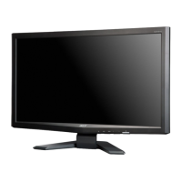
ACER X203W

 Loading...