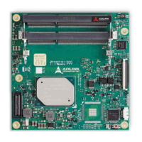
cExpress-AL
Pinouts and Signal Descriptions 21
SD/GPIO Pin Mapping
GPIO Signal SD Signal Note
GPI0 SD_DATA0 Bidirectional signal
GPI1 SD_DATA1 Bidirectional signal
GPI2 SD_DATA2 Bidirectional signal
GPI3 SD_DATA3 Bidirectional signal
GPO0 SD_CLK Output from COM Express, input to SD
GPO1 SD_CMD Output from COM Express, input to SD
GPO2 SD_WP Input to COM Express when used as SD_WP
GPO3 SD_CD# Input to COM Express when used as SD_CD#
3.3.15. Serial Interface Signals
Signal Pin Description I/O PU/PD Comment
SER0_TX A98
General purpose serial port transmitter (TTL level
output)
O CMOS PU 1k 5V
Power rail tolerance
5V/12V
There shall be PD on
carrier board
SER0_RX A99
General purpose serial port receiver (TTL level
input)
I CMOS
PU 4.7k
5V
Power rail tolerance
5V/12V
SER1_TX A101
General purpose serial port transmitter (TTL level
output)
O CMOS PU 1k 5V
Power rail tolerance
5V/12V
There shall be PD on
carrier board
SER1_RX A102
General purpose serial port receiver (TTL level
input)
I CMOS
PU 4.7k
5V
Power rail tolerance
5V/12V
3.3.16. Power And System Management
Signal Pin Description I/O PU/PD Comment
PWRBTN# B12
Power button to bring system out of S5 (soft off), active
on falling edge.
I 3.3VSB
PU 10k
3.3VSB
SYS_RESET# B49
Reset button input. Active low request for module to
reset and reboot. May be falling edge sensitive. For
situations when SYS_RESET# is not able to reestablish
control of the system, PWR_OK or a power cycle may
be used.
I 3.3VSB
PU 10k
3.3VSB
CB_RESET# B50
Reset output from module to Carrier Board. Active low.
Issued by module chipset and may result from a low
SYS_RESET# input, a low PWR_OK input, a VCC_12V
power input that falls below the minimum specification, a
watchdog timeout, or may be initiated by the module
software.
O 3.3VSB
PWR_OK B24
Power OK from main power supply. A high value
indicates that the power is good. This signal can be
used to hold off Module startup to allow carrier based
FPGAs or other configurable devices time to be
programmed.
I 3.3V
PU 10k
3.3V
 Loading...