20 Registers
3.2 I/O Address Map
All 725X registers are 8 bits long. Users can access these regis-
ters using 8-bit I/O instructions. Using these registers will allow the
relays and status of the inputs to be controlled. The following table
shows the registers address map, including descriptions and their
offset addresses relative to the base address. If the PCI-7251
expansion boards are not installed, corresponding registers have
no significance.
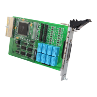
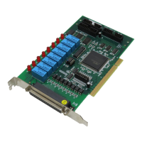
3.3 Relay Output and Readback Registers
There are 8 relays on each PCI-7250 / 7251 and cPCI-7252
board. Each relay is controlled by one bit in the control register. Bit
value ‘0’ means the relay is not energized. The normal open signal
line is ‘open’. Bit value ‘1’ means the relay is energized and the
normal open signal line is now closed.
The initial bit values of the control register are all ‘0’ and the status
of the relay can be readback from the readback register. If the
Offset Write Read Board
0 Relay Output Output readback
PCI-7250
1 Not used Isolation Input
2 Relay Output Output readback
PCI-7251 #1
3 Not used Isolation Input
4 Relay Output Output readback
PCI-7251 #2
5 Not used Isolation Input
6 Relay Output Output readback
PCI-7251 #3
7 Not used Isolation Input
Table 3-1: PCI-7250 Address Map with PCI-7251 Installed
Offset Write Read Board
0 Relay Output Isolation Input
cPCI-72521 Not used Not used
2 Not used Output readback
Table 3-2: cPCI-7252 Address Map
 Loading...