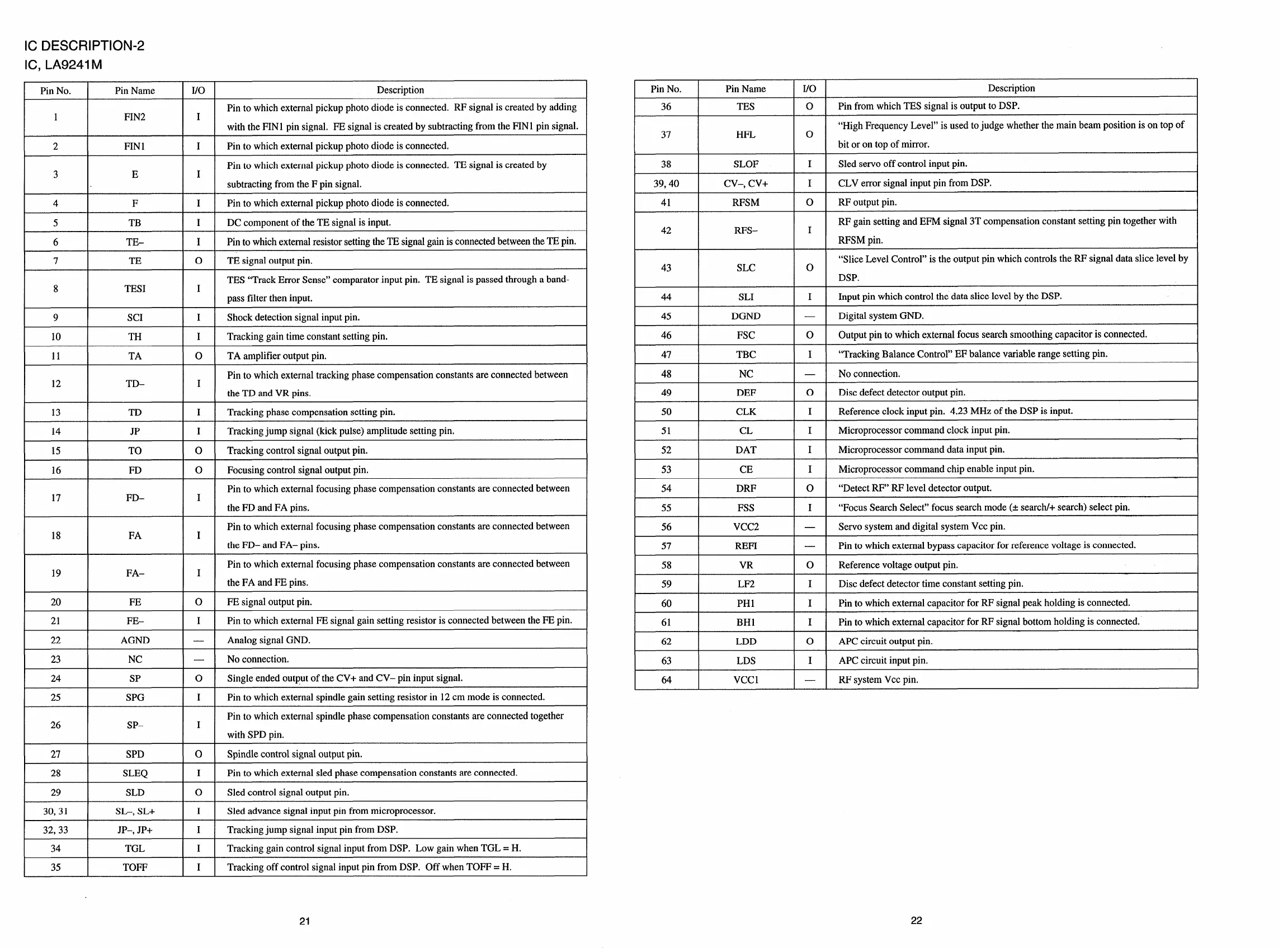
Ic DESCRIPTION-2
IC, LA9241 M
Pin No.
Pin Name
I/o
Description
Pin to which external pickup photo diode is connected. RF signal is created by adding
1 FIN2
I
Pin No.
Pin Name
I/o
Description
36
TES
o
Pin from which TES signal is output to DSP.
“High Frequency Level” is used to judge whether the main beam position is on top of
37 HFL o
1 I
I with the FIN1 pin signal, FE signal is created by subtracting from the FIN1 pin signal.
I I I
I bit or on top of mirror. I
2
I
FIN1
I I I Pinto which external pickup photo diode is connected,
I
38
I
SLOF
I
I
I
Sled servo off control input pin.
I
3
I I
I
Pin to which external pickup photo diode is connected, TE signal is created by
I
E
I
I
39,40 I
Cv–, Cv+
I
I I CLV error signal input pin from DSP.
I subtracting from the F pin signal,
II
I
Pin to which external pickup photo diode is connected,
I
41
I
RFSM
I O I RF output pin,
4
IF
RF gain setting and EFM signal 3T compensation constant setting pin together with
I
42
I
I
DC component of the TE signal is input.5 TB
6 TE-
RFS-
RFSM pin.
1 1
1
I
I
I
Pin to which external resistor setting the TE signal gain is connected between the TE pin.
I I I
I
“Slice Level Control” is the output pin which controls the RF signal data slice level by
43 SLC o
I
o
I
TE signal output pin.
7
I
TE
I
I I
I DSP.
I I
I
TES “Track Error Sense” comparator input pin. TE signal is passed through a band-
8
TESI
1
I
44
I
SLI
I
1
I
Input pin which control the data slice level by the DSP.
I
pass filter then input.
I
Shock detection signal input pin.
I
45
I
DGND
I
—
I
Digital system GND.
I9
I
SCI
I
46
I
FSC
I
o
I
Output pin to which external focus search smoothing capacitor is connected.
I
I
I
Tracking gain time constant setting pin.
I
47
I
TBC
I
I
I
“Tracking Balance Control” EF balance variable range setting pin.
I
O I TA amplifier output pin.
I
48
I
NC
I
—
I
No connection,
I
I
Pin to which external tracking phase compensation constants are connected between
I
12
I
TD-
1
49
I
DEF
I O I Disc defect detector output pin.
I
the TD and VR pins.
I
Tracking phase compensation setting pin.
I
50
I
CLK
] I I Reference clock input pin. 4.23 MHz of the DSP is input.
I
-H----
I
51
I
CL
I
1
I
Microprocessor command clock input pin.
I
I
I
Tracking jump signal (kick pulse) amplitude setting pin,
I
52
I
DAT
I
I
I
Microprocessor command data input pin.
I
15
I
TO
I O I Tracking control signal output pin.
I
53
I
CE
I
I
I
Microprocessor command chip enable input pin.
I
16
I
FD I O I Focusing control signal output pin.
I
54
I
DRF
I
o
I
“Detect RF” RF level detector output.
I
17 FD-
Pin to which external focusing phase compensation constants are connected between
I
the FD and FA pins.
I
55
I
FSS
I
I
I
“Focus Search Select” focus search mode (* search/+ search) select pin.
I
56
VCC2
—
Servo system and digital system Vcc pin.
57 REFI
—
Pin to which external bypass capacitor for reference voltage is connected.
58
VR
o
Reference voltage output pin.
18 FA
Pin to which external focusing phase compensation constants are connected between
I
the FD– and FA– pins.
19
Pin to which external focusing phase compensation constants are connected between
I
the FA and FE pins.
FA-
1
59
I
LF2 I I I Disc defect detector time constant setting pin.
I
20
I
FE
I
o
I
FE
signal output pin.
I
60
I
PH1
I
I
I
Pin to which external capacitor for RF signal peak holding is connected.
I
I
I
Pin to which external FE signal gain setting resistor is connected between the FE pin.
I
61
I
BH1
I
I
I
Pin to which external capacitor for RF signal bottom holding is connected.
I
I
62
I
LDD
I
o
I
APC circuit output pin.
I
22
I
AGND
– I Analog signal GND.
I
63
I
LDS
I
I
I
APC circuit input pin.
I
23
I
NC
– I No connection.
o
I
Single ended output of the CV+ and CV– pin input signal.
I
64
I
Vccl
I
—
I
RF system Vcc pin.
I
-+-w-
1
I
Pin to which external spindle gain setting resistor in 12cm mode is connected.
26
I
I
I
Pin to which external spindle phase compensation constants are connected together
I
sP-
1 I
I with SPD pin.
27
I
SPD
I
o
I
Spindle control signal output pin.
28
I
SLEQ
I
I
I
Pin to which external sled phase compensation constants are connected.
29
I
SLD
I
o
I
Sled control signal output pin.
30,31
I
SL-, SL+
I
I I Sled advance signal input pin from microprocessor.
32,33
I
JP–, JPi-
1
1
I
Tracking jump signal input pin from DSP.
34
I
TGL
I I I Tracking gain control signal input from DSP. Low gain when TGL = H.
35
I
TOFF
I I I Tracking off control signal input pin from DSP. Off when TOFF = H.
21
22
 Loading...