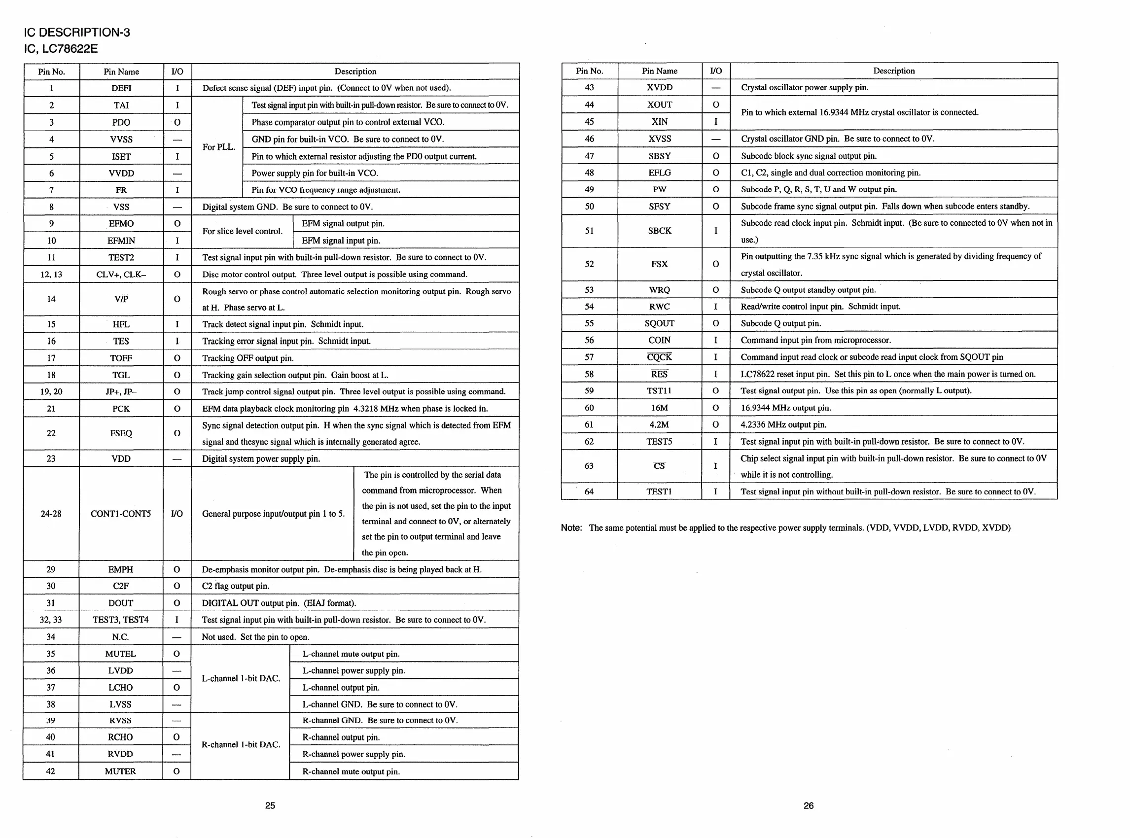
Ic DESCRIPTION-3
IC, LC78622E
Pin No.
Pin Name
I/o
Description
1 DEFI
I
Defect sense signal (DEF) input pin. (Connect to OVwhen notused).
2
TAI
I Testsignalinputpinwithbuilt-inpull-downm.sister.Be suretoconnecttoOV.
3 PDO o
Phase comparator output pin to control external VCO.
4 Vvss
—
GND pin for built-in VCO. Be sure to connect to OV.
For PLL.
5 ISET I
Pin to which external resistor adjusting the PDOoutput current.
6 VVDD
—
Power supply pin for built-in VCO.
7
FR
I
Pin for VCO frequency range adjustment,
8
Vss
—
Digital system GND. Besureto connect toOV.
9
EFMO o EFM signal output pin.
For slice level control.
10
EFMIN
I EFM signal input pin.
11
TEST2
I
Testsignal input pinwith built-in pull-down resistor, Besureto connect toOV.
12, 13 CLV+, CLK- 0
Disc motor control output, l%reelevel output impossibleusing command.
Rough servo or phase control automatic selection monitoring output pin, Rough servo
14 VF
o
at H. Phase servo at L.
15
HFL
I
Track detect signal input pin. Schmidt input.
16 TES I Tracking error signal input pin. Schmidt input.
17 TOFF o Tracking OFF output pin,
18
TGL o
Tracking gain selection output pin. Gain boost at L.
19,20 JP+, JP– 0
Track jump control signal output pin. Three level output is possible using command.
21
PCK
o EFM data playback clock monitoring pin 4.3218 MHz when phase is locked in.
Sync signal detection output pin. H when the sync signal which is detected from EFM
22 FSEQ
o
signal and thesync signal which is internally generated agree,
23 VDD
—
Digital system power supply pin.
The pin is controlled by the serial data
command from microprocessor. When
the pin is not used, set the pinto the input
24-28 CONT1-CONT5 I/o General purpose input/output pin 1 to 5.
terminal and connect to OV,or alternately
set the pin to output terminal and leave
the pin open.
29
EMPH o De-emphasis monitor output pin. De-emphasis disc is being played back at H.
30 C2F o C2 flag output pin,
31 DOUT o
DIGITAL OUT output pin, (EIAJ format).
32,33
TEST3, TEST4
I
Test signal input pin with built-in pull-down resistor. Be sure to connect to OV.
34 N.C.
—
Not used. Set the pin to open.
35 MUTEL o
L-channel mute output pin.
36 LVDD
—
L-channel power supply pin.
L-channel l-bit DAC.
37 LCHO o L-channel output pin.
38 LVSS
—
L-channel GND. Be sure to connect to OV,
39 RVSS
—
R-channel GND. Be sure to connect to OV,
40
RCHO o R-channel output pin.
R-channel l-bit DAC.
41
RVDD — R-channel power supply pin.
42
MUTER
o R-channel mute output pin.
Pin No. Pin Name
I/o
Description
43 XVDD
—
Crystal oscillator power supply pin.
44 XOUT o
Pin to which external 16.9344 MHz crystal oscillator is connected.
45 XIN I
I
46
I
Xvss
I
—
I
Crystal oscillator GND pin. Be sure to connect to OV.
I
I
47
I
SBSY
I
o
I
Subcode block sync signal output pin,
I
I
48
I
EFLG I O I Cl, C2, single and dual correction monitoring pin.
I
49 Pw o Subcode P, Q, R, S, T, U and W output pin.
50 SFSY o Subcode frame sync signal output pin. Falls down when subcode enters standby.
Subcode read clock input pin. Schmidt input. (Be sure to connected to OVwhen not in
51
SBCK
I
use.)
Pin outputting the 7.35 kHz sync signal which is generated by dividing frequency of
52 FSX o
crystal oscillator.
53 WRQ o Subcode Q output standby output pin.
54
RWC
I Read/write control input pin. Schmidt input.
I
55
I
SQOUT
I
o
I
Subcode Q output pin.
I
I
56
I
COIN
I I I Command input pin from microprocessor.
I
57
CQCK
I
Command input read clock or subcode read input clock from SQOUT pin
58 REs I LC78622 reset input pin. Set this pinto L once when the main power is turned on.
59 TST11 o Test signal output pin. Use this pin as open (normally L output).
60 16M o
16.9344 MHz output pin.
61 4.2M o 4.2336 MHz output pin.
62 TEST5 I Test signal input pin with built-in pull-down resistor. Be sure to connect to OV.
Chip select signal input pin with built-in pull-down resistor. Be sure to connect to OV
63 Cs
I
while it is not controlling.
64 TEST1
I
Test signal input pin without built-in pull-down resistor. Be sure to connect to OV.
Note: The same potential must be applied to the respective power supply terminals. (VDD, VVDD, LVDD, RVDD, XVDD)
25 26
 Loading...