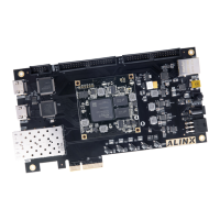
The ARTIX-7 FPGA Development Board AX7203 is a versatile platform designed for high-speed data processing, video transmission, and industrial control applications. It adopts a core board + carrier board architecture, facilitating secondary development.
Function Description:
The AX7203 serves as a comprehensive development platform for Xilinx Artix-7 FPGAs. The core board, AC7200, is centered around the XC7A200T chip in a BGA 484 package, providing high speed, bandwidth, and capacity. It handles high-speed data processing and storage, with efficient data reading and writing between the FPGA and two DDR3 modules. The carrier board expands the core board's capabilities by offering a rich set of peripheral interfaces, making it suitable for a wide range of applications including PCIe high-speed data exchange, video processing, network communication, and data processing. It is an ideal tool for students, engineers, and anyone involved in Artix-7 FPGA development.
Important Technical Specifications:
Core Board (AC7200):
- FPGA: Xilinx Artix-7 XC7A200T-2FGG484I (BGA 484 package)
- Logic Cells: 215360
- Slices: 33650
- CLB flip-flops: 269200
- Block RAM (kb): 13140
- DSP Slices: 740
- PCIe Gen2: 1
- XADC: 1 XADC, 12bit, 1Mbps AD
- GTP Transceiver: 4 GTP, 6.6Gb/s max
- Speed Grade: -2 (Industrial)
- DDR3 DRAM: 2x Micron MT41J256M16HA-125 (compatible with MT41K256M16HA-125)
- Capacity: 8Gbit (2x 4Gbit)
- Data Bus Width: 32-bit
- Max Operating Speed: 800MHz (1600Mbps data rate)
- Bandwidth: Up to 25Gb/s
- QSPI Flash: 1x 128MBit W25Q256FVEI
- Voltage Standard: 3.3V CMOS
- Function: Boot device for system images (FPGA bit files, ARM application code, user data)
- Clocks:
- 200MHz active differential crystal (SiT9102-200.00MHz) for FPGA system clock and DDR3 control.
- 125MHz active differential crystal (SiT9102-125MHz) for GTP transceivers reference clock.
- IO Ports: 180 standard 3.3V IOs, 15 standard 1.5V IOs, 4 pairs of GTP high-speed RX/TX differential signals.
- Board-to-Board Connectors: Four 80-pin 0.5mm pitch connectors for high-speed data communication with the carrier board.
- CON1: Connects to VCCIN (+5V), ground, and normal FPGA IOs (15 pins connected to BANK34 for DDR3, 1.5V standard).
- CON2: Extends normal IOs of BANK13 and BANK14 (3.3V standard).
- CON3: Extends normal IOs of BANK15 and BANK16 (3.3V standard, adjustable via LDO), and four JTAG signals.
- CON4: Extends normal IO and GTP high-speed data and clock signals of FPGA BANK16 (3.3V standard, adjustable via LDO).
- Power Supply: DC5V input (via carrier board or J3 for standalone use). Four DC/DC power supply chips (TLV62130RGT) convert to +3.3V, +1.5V, +1.8V, +1.0V (up to 3A per channel). VCCIO for BANK15/16 generated by LDOSPX3819M5-3-3. VTT and VREF for DDR3 generated by TI's TPS51200. MGTAVTT and MGTAVCC for GTP transceiver generated by TI's TPS74801.
- +1.0V: FPGA Core Voltage
- +1.8V: FPGA auxiliary power supply, TPS74801 power supply
- +3.3V: VCCIO of Bank0, Bank13 and Bank14 of FPGA, QSPIF FLASH, Clock Crystal
- +1.5V: DDR3, Bank34 and Bank35 of FPGA
- VREF, VTT (+0.75V): DDR3
- MVCCIP (+3.3V): FPGA Bank15, Bank16
- MGTAVTT (+1.2V): GTP Transceiver Bank216 of FPGA
- MGTVCCAUX (+1.8V): GTP Transceiver Bank216 of FPGA
- Dimensions: 45mm x 55mm
Carrier Board:
- PCIe Interface: 1x PCIe x4 interface (PCI Express 2.0 standard)
- Communication Rate: Up to 5G Baud per channel
- Reference Clock: 100MHz (from PCle slot)
- Ethernet Interfaces: 2x Gigabit Ethernet RJ-45 interfaces
- Chip: Micrel KSZ9031RNX Ethernet PHY
- Rates: 10/100/1000 Mbps (full duplex, adaptive)
- Communication Bus: GMII
- HDMI Interfaces:
- 1x HDMI Output interface (Silion Image SIL9134 encoding chip)
- Output: Up to 1080P@60Hz, supports 3D output.
- 1x HDMI Input interface (Silion Image SIL9013 decoder chip)
- Input: Up to 1080P@60Hz, supports data output in various formats.
- USB to Serial Port: 1x Uart to USB interface (Mini USB)
- Chip: Silicon Labs CP2102GM
- SD Card Slot: 1x Micro SD card holder (supports SD mode and SPI mode)
- EEPROM: Onboard 1x IIC interface EEPROM 24LC04 (4Kbit capacity)
- Expansion Headers: 2x 40-pin 2.54mm pitch expansion ports (J11, J13)
- Signals: 1x 5V power, 2x 3.3V power, 3x ground, 34 IOs.
- JTAG Interface: 1x 10-pin 0.1inch spacing standard JTAG port for FPGA program download and debugging.
- XADC Interface: (Not installed by default) Extends three pairs of ADC differential input interfaces to the FPGA's 12-Bit 1Msps analog-to-digital converter.
- Keys: 2 user keys (KEY1, KEY2) on carrier board, 1 reset key on core board.
- LED Lights: 5 user LEDs (1 on core board, 4 on carrier board), 1 power indicator (PWR), 2 USB Uart data indicators (TX, RX).
- Power Input: DC12V (via adapter, PCIe interface, or ATX chassis power supply).
- Power Supply (Carrier Board): 4-channel DC/DC power supply chip MP1482 converts +12V to +5V, +3.3V, +1.8V, +1.2V. +5V also powers the AC7100B core board.
Usage Features:
- Modular Design: The core board + carrier board architecture allows for flexible development. Users can utilize the core board for secondary development or leverage the carrier board's extensive peripherals.
- High-Speed Data Handling: With DDR3 memory and GTP transceivers, the board is well-suited for applications requiring high bandwidth and fast data transfer, such as fiber-optic communications and PCIe data communications.
- Video Processing Capabilities: Dedicated HDMI input and output interfaces, along with the FPGA's processing power, enable video transmission and processing applications.
- Network Connectivity: Dual Gigabit Ethernet interfaces provide robust network communication services.
- Expandability: Two 40-pin expansion headers allow connection to various ALINX modules (e.g., binocular cameras, TFT LCD screens, high-speed AD modules) or custom external circuits.
- Debugging and Programming: Standard JTAG interfaces on both the core board and carrier board facilitate FPGA program download and debugging. A USB-to-serial port simplifies communication with a host PC for debugging.
- Boot Device: The QSPI Flash acts as a non-volatile boot device for storing system images, including FPGA bit files and application code.
- Flexible Powering: The board can be powered via a DC12V adapter, the PCIe interface, or an ATX chassis power supply.
Maintenance Features:
- Power-Up Sequence: The Artix-7 FPGA system requires a specific power-up sequence (VCCINT -> VCCBRAM -> VCCAUX -> VCCO) and a reversed power-off sequence to prevent damage. For GTP transceivers, the sequence is VCCINT -> VMGTAVCC -> VMGTAVTT. If voltages are the same, they can be powered up simultaneously.
- IO Voltage Standards: Be aware of the different voltage standards for FPGA banks (e.g., BANK34 for DDR3 is 1.5V, others are 3.3V). The voltage standards for BANK15 and BANK16 on CON3 and BANK16 on CON4 can be adjusted by replacing the LDO chip.
- Expansion Port Protection: A 33-ohm resistor is connected in series between the expansion port and the FPGA to protect against external voltage or current. However, direct connection of 5V devices to the IOs is not recommended without a level conversion chip to avoid burning the FPGA.
- JTAG Hot Swapping: Avoid hot-swapping the JTAG cable to prevent damage to the FPGA chip. Protection diodes are included in the JTAG signal path to ensure voltage levels are within the FPGA's acceptable range.
- Power Conflict Prevention: When using the core board alone, power should be supplied only via the J3 interface. Do not simultaneously power the core board via J3 and the carrier board to avoid current conflicts and potential damage.
- Signal Integrity: The DDR3 memory system is designed with strict signal integrity considerations, including matching resistor/terminal resistance, trace impedance control, and trace length control, to ensure stable high-speed operation.