2.2 Headers
The board exposes two 15 pin connectors which can either be assembled with pin headers or soldered through
castellated vias.
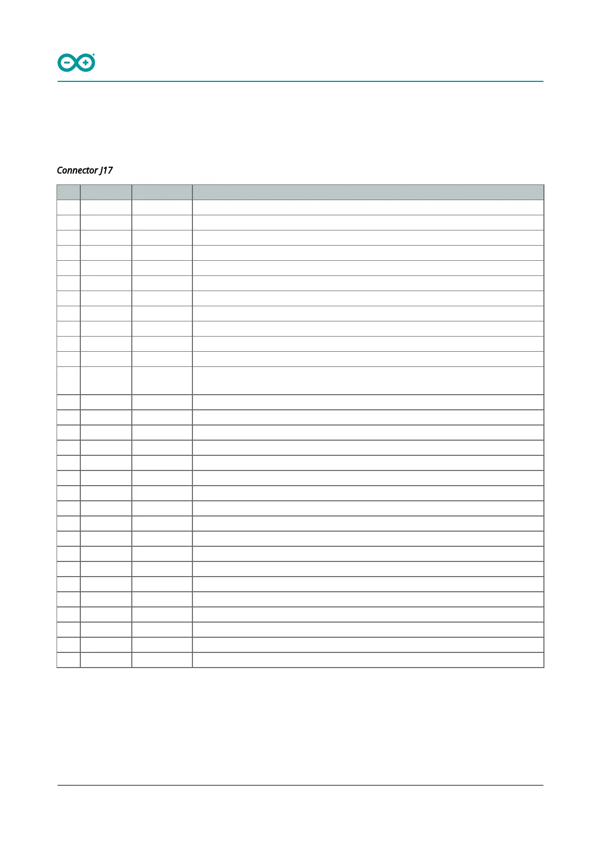
Connector J17
Pin Function Type Description
1 D13/SCK Digital GPIO
2 +3V3 Power Out
3 AREF Analog Analog Reference; can be used as GPIO
4 A0/DAC0 Analog ADC in/DAC out; can be used as GPIO
5 A1 Analog ADC in; can be used as GPIO
6 A2 Analog ADC in; can be used as GPIO
7 A3 Analog ADC in; can be used as GPIO
8 A4/SDA Analog ADC in; I2C SDA; Can be used as GPIO (1)
9 A5/SCL Analog ADC in; I2C SCL; Can be used as GPIO (1)
10 A6 Analog ADC in; can be used as GPIO
11 A7 Analog ADC in; can be used as GPIO
12 VUSB
Power
In/Out
Normally NC; can be connected to VUSB pin of the USB connector by shorting a
jumper
13 RST Digital In Active low reset input (duplicate of pin 18)
14 GND Power Power Ground
15 VIN Power In Vin Power input
16 TX Digital USART TX; can be used as GPIO
17 RX Digital USART RX; can be used as GPIO
18 RST Digital Active low reset input (duplicate of pin 13)
19 GND Power Power Ground
20 D2 Digital GPIO
21 D3 Digital GPIO
22 D4 Digital GPIO
23 D5 Digital GPIO
24 D6 Digital GPIO
25 D7 Digital GPIO
26 D8 Digital GPIO
27 D9 Digital GPIO
28 D10 Digital GPIO
29 D11/MOSI Digital SPI MOSI; can be used as GPIO
30 D12/MISO Digital SPI MISO; can be used as GPIO
 Loading...