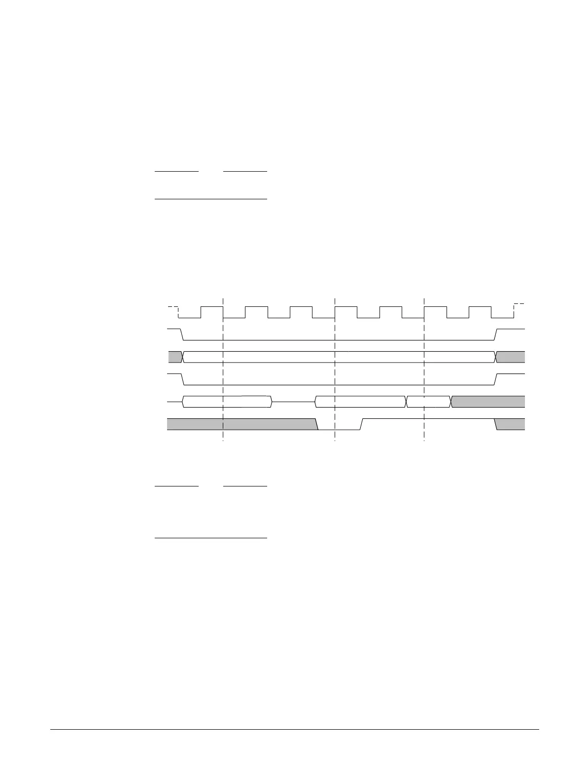
Address and data transfer out of the MCC‑SMC interface
The MCC provides 25 of the 32 bits that the FPGA design uses for AHB‑type transactions. The
FPGA design generates the other 7 bits.
During the address phase, the 25 address bits are shared between SMBM_D[15:0] and
SMBM_A[24:16].
• SMBM_D[15:0] carries the 16 least significant address bits of the interface.
• SMBM_A[24:16] carries the nine most significant address bits of the interface.
Note
SMBM_A[25] is not used.
During the data transfer phase, SMBM_D[15:0] carries the four data bytes in two stages. It
carries the two least significant bytes, and then the two most significant data bytes.
The following figure shows an MCC‑SMC interface address and data transfer.
SMBM_CLK
READ/WRITE
ADDRESS
READ/WRITE DATA
Two least
significant bytes
SMBM_nEx
SMBM_A[25:16]
SMBM_nWE
SMBM_D[15:0]
SMBM_nWAIT
A[15:0]
D[15:0]
A[24:16]
READ/WRITE DATA
Two most
significant bytes
D[31:16]
Figure 2-10 MCC-SMC interface address and data transfer timing
Note
• The MCC-SMC interface supports only 32‑bit data read and write transfers.
• To meet the timing requirements for address and data transfer, Arm recommends that you
use the MCC‑SMC interface decoder in the file microToAhb.v, provided by Arm.
2 Hardware description
2.7 MCC-SMC interface
100765_0000_04_en Copyright © 2017–2020 Arm Limited or its affiliates. All rights
reserved.
2-31
Non-Confidential