Forming the 32-bit address in the FPGA
The FPGA design must form the 32‑bit address, for AHB‑ type transfers inside the FPGA, from
the following:
• The least significant bit (LSB), generated by the FPGA design.
Note
The MCC-SMC interface supports only four‑byte address mode transactions. To support
four‑byte address mode, the LSB generated by the FPGA design must be 0b0 and the LSB of
the MCC-SMC interface is always 0b0.
• 25 address bits from the MCC.
• Six user bits, generated by the FPGA design.
The MCC can access 64MB of user memory for each Chip‑Select, that is, a total memory space
of 256MB. Each Chip‑Select can point to non‑contiguous areas in the user design. But the total
amount of user memory that each Chip‑Select accesses cannot exceed 64MB.
The six address bits generated by the design, and if necessary, the Chip‑Select bits, define which
parts of the user memory space are accessed.
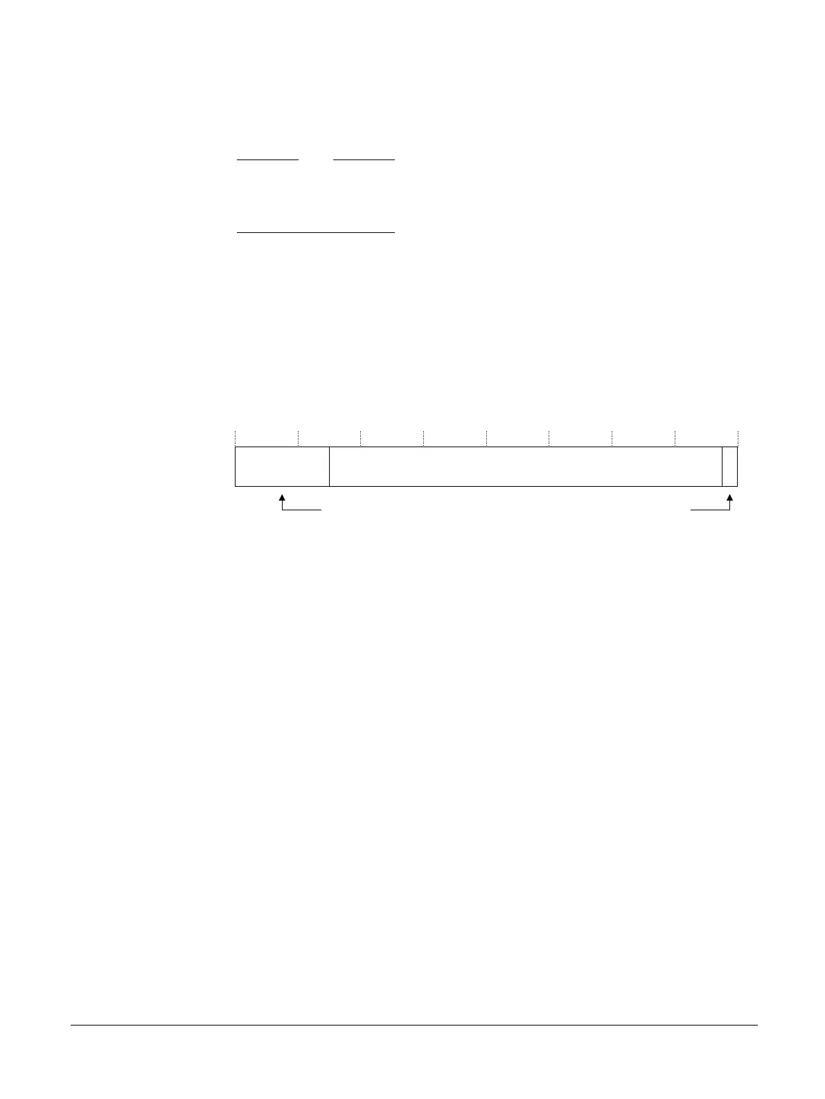
The following figure shows the formation of the AHB 32‑bit address in the FPGA.
31 1 0
6 user bits 0
26 25
User bits generated
by FPGA design from
Chip-Selects and user
defined offsets
LSB generated
by FPGA design
SMBM_A[24:16],SMBM_D[15:0]
Figure 2-11 Formation of 32-bit address in FPGA
2 Hardware description
2.7 MCC-SMC interface
100765_0000_04_en Copyright © 2017–2020 Arm Limited or its affiliates. All rights
reserved.
2-32
Non-Confidential