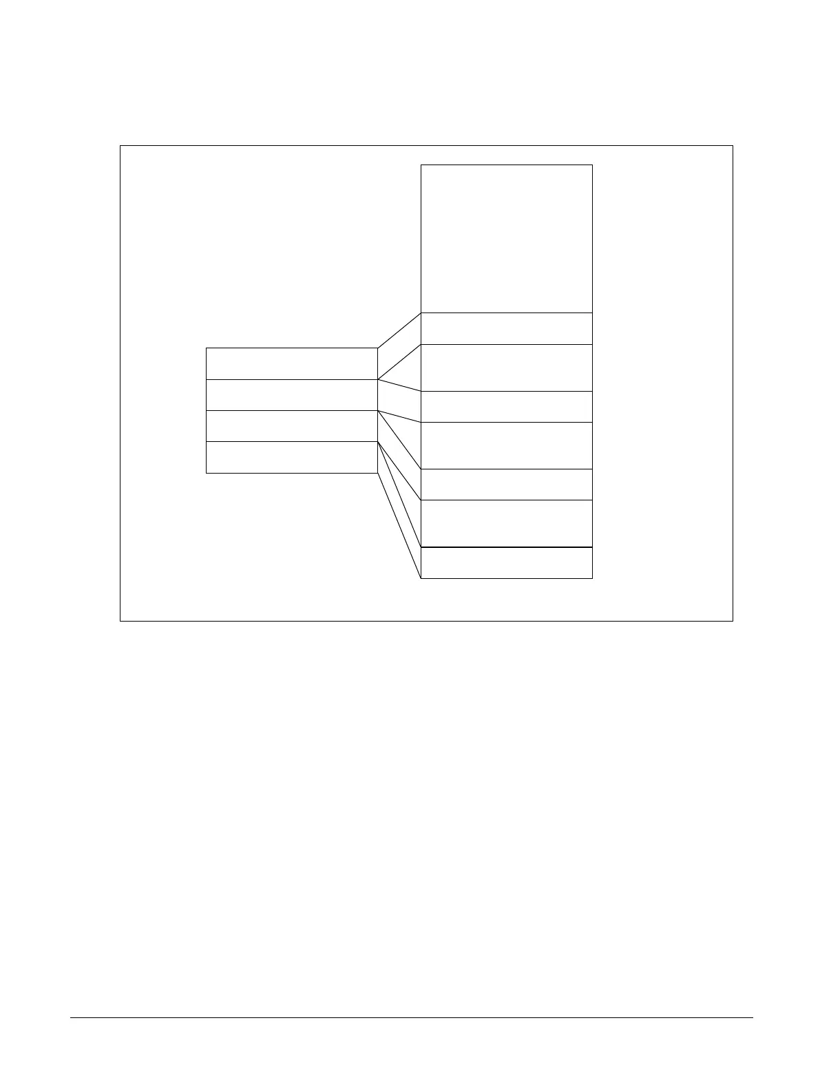
Example user memory map
The following figure shows an example user memory map.
0x0000_0000
0x03FF_FFFF
MCC memory
Chip-Select 0-64MB
Chip-Select 1-64MB
Chip-Select 2-64MB
Chip-Select 3-64MB
0x0000_0000
0x03FF_FFFF
0xFFFF_FFFF
FPGA user memory map
SMBM_nE[4:1]=0xE
SMBM_nE[4:1]=0xD
0x0C00_0000
0x0FFF_FFFF
0x3000_0000
0x33FF_FFFF
0xC000_0000
0xC3FF_FFFF
SMBM_nE[4:1]=0xB
SMBM_nE[4:1]=0x7
0x0C00_0000
0x0FFF_FFFF
0x0800_0000
0x0BFF_FFFF
0x0400_0000
0x07FF_FFFF
Figure 2-12 Example user memory map
The example memory map shows the mapping when the six user bits have the following values
for each Chip‑Select:
• CS0:
— The image in the FPGA generates internal AHB address bits[31:26] =0b000000 which
gives a base address of 0x00000000.
• CS1:
— The image in the FPGA generates internal AHB address bits[31:26] =0b000011 which
gives a base address of 0x0C000000.
• CS2:
— The image in the FPGA generates internal AHB address bits[31:26] =0b001100 which
gives a base address of 0x30000000.
• CS3:
— The image in the FPGA generates internal AHB address bits[31:26] =0b110000 which
gives a base address of 0xC0000000.
The variable IMAGE0ADDRESS in the images.txt configuration file defines the base address
in the MCC memory. In this example, setting IMAGE0ADDRESS to 0x05000000 selects a base
address of 0x0D000000 in the FPGA user memory. The firmware sets SMBM_nE[4:1] to 0xD to
select Chip‑Select 1 which maps to the correct area of user memory.
2 Hardware description
2.7 MCC-SMC interface
100765_0000_04_en Copyright © 2017–2020 Arm Limited or its affiliates. All rights
reserved.
2-33
Non-Confidential