The following table shows the pin mapping for each P‑JTAG, SWD, and 16‑bit trace signal on the 20‑pin
Cortex debug and ETM connector.
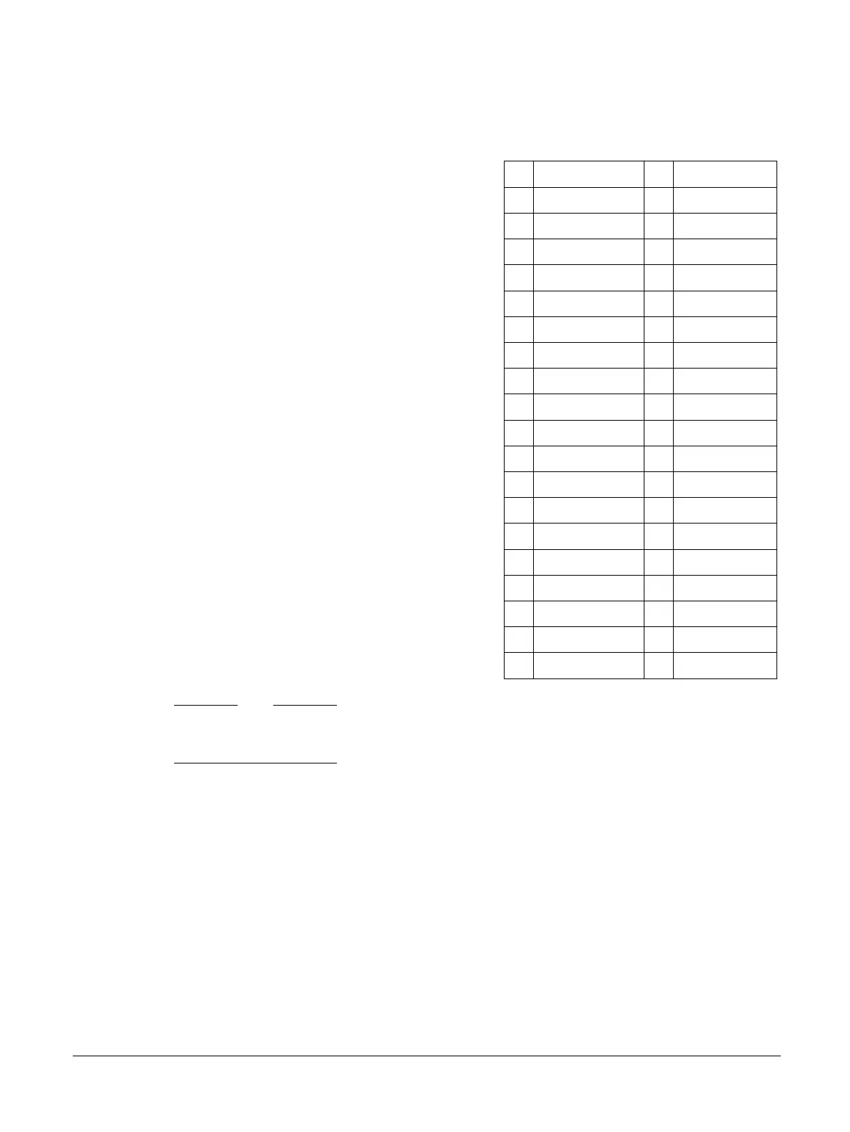
Table A-4 38-pin MICTOR connector, J13, pin mapping
Pin Signal Pin Signal
1 NC 2 NC
3 NC 4 NC
5 GND 6 TRACECLK
7 DBGRQ 8 DBGACK
9 NC/nSRST 10 EXTTRIG
11 TDO/SWO 12 1V8 reference
13 RTCK 14 1V8_OUT
15 TCK/SWCLK 16 TRACEDATA[7]
17 TMS/SWDIO 18 TRACEDATA[6]
19 TDI 20 TRACEDATA[5]
21 nTRST 22 TRACEDATA[4]
23 TRACEDATA[15] 24 TRACEDATA[3]
25 TRACEDATA[14] 26 TRACEDATA[2]
27 TRACEDATA[13] 28 TRACEDATA[1]
29 TRACEDATA[12] 30 GND
31 TRACEDATA[11] 32 GNDDETECT
33 TRACEDATA[10] 34 1V8 reference
35 TRACEDATA[9] 36 TRACECTL
37 TRACEDATA[8] 38 TRACEDATA[0]
Note
• Pins 9, 11, 17, 19, and 21 have pullup resistors to 1V8.
• Pins 13 and 15 have pulldown resistors to GND.
Related information
2.18 System debug on page 2-50
1.3 Location of components on the MPS3 board on page 1-15
A.1.5 14-pin F-JTAG ILA connector
The MPS3 board provides one 3V3 14‑pin F‑JTAG ILA connector that supports FPGA debug. It enables
you to connect an ILA device, such as SignalTap II, to a hard FPGA JTAG chain in the FPGA and debug
your design.
The following figure shows the 14‑pin F‑JTAG ILA connector, J17.
A Signal descriptions
A.1 Debug connectors
100765_0000_04_en Copyright © 2017–2020 Arm Limited or its affiliates. All rights
reserved.
Appx-A-74
Non-Confidential