See 1.3 Location of components on the MPS3 board on page 1-15 for the location of the Arduino Shield
interface connectors on the MPS3 board.
Note
User‑links select digital I/O operating voltages and power inputs. The power inputs and IOREF voltages
have maximum current limits available at the board interface pins. See 2.16 Arduino Shield and Pmod
interfaces on page 2-43 for information on the user‑links, and the maximum available IOREF currents.
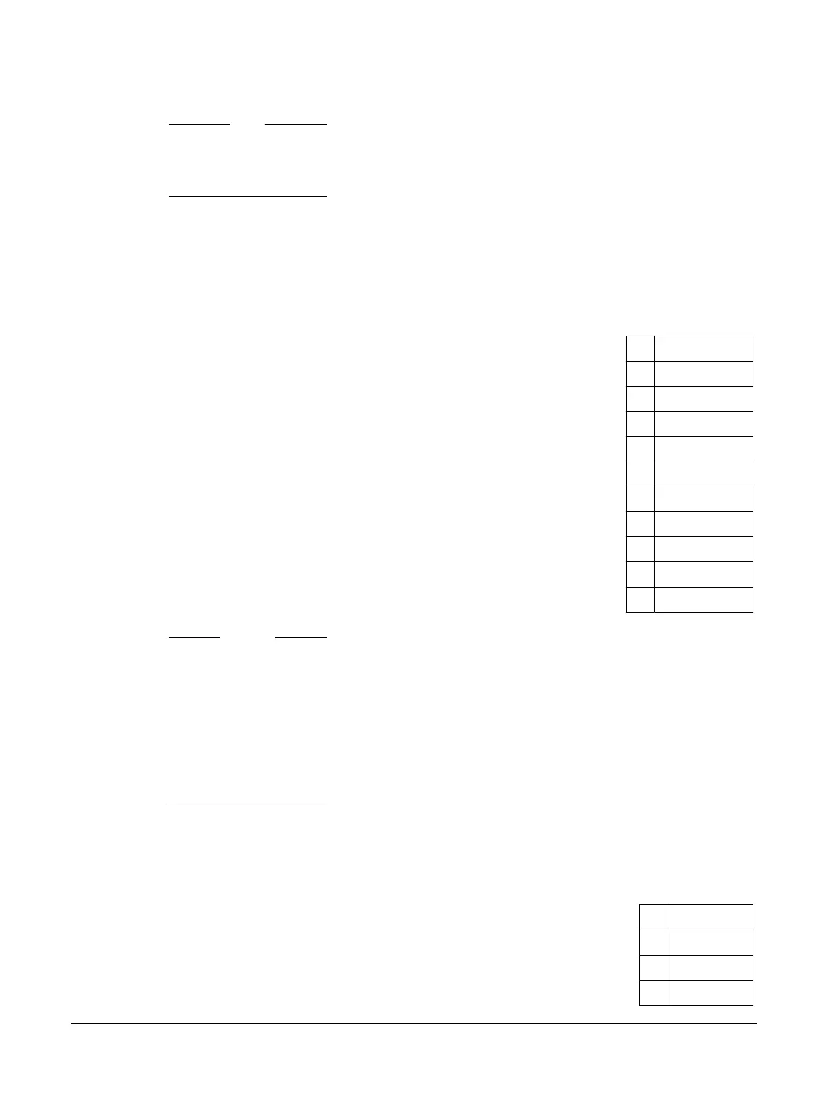
Digital I/O connectors: Connectors J25, J33, J30, and J39
Connector J25 provides Shield 0 I/O[15:8], and connector J33 provides Shield 1 I/O[15:8]. The
connectors also provide the analog I/O reference voltages. The following table shows the pin mapping
for connectors J25 and J33.
Table A-6 Connectors J25 (Shield 0) and J33 (Shield 1) signal list
Pin Signal
1 SH0/SH1_IO8
2 SH0/SH1_IO9
3 SH0/SH1_IO10
4 SH0/SH1_IO11
5 SH0/SH1_IO12
6 SH0/SH1_IO13
7 GND
8 SH0/SH1_AREF
9 SH0/SH1_IO14
10 SH0/SH1_IO15
Caution
FPGA pins SH0_IO16, SH0IO17, SH1_IO16, and SH1_IO17, which are unused, connect to the Shield
connectors through 4K7 resistors.
• FPGA pin SH0_IO16 connects to Shield pin SH0_IO14.
• FPGA pin SH0_IO17 connects to Shield pin SH0_IO15.
• FPGA pin SH1_IO16 connects to Shield pin SH1_IO14.
• FPGA pin SH1_IO17 connects to Shield pin SH1_IO15.
Arm recommends that you set FPGA pins SH[1:0]_IO[17:16] to high impedance to prevent any
possibility of interference with connector pins SH[1:0]_IO[15:14].
Connector J30 provides Shield 0 I/O[7:0] and connector J36 provides Shield 1 I/O[7:0]. The following
table shows the pin mapping for connectors J30 and J36.
Table A-7 Connectors J30 (Shield 0) and J36 (Shield 1) signal list
Pin Signal
1 SH0/SH1_IO0
2 SH0/SH1_IO1
3 SH0/SH1_IO2
A Signal descriptions
A.2 Arduino Shield connectors
100765_0000_04_en Copyright © 2017–2020 Arm Limited or its affiliates. All rights
reserved.
Appx-A-77
Non-Confidential