2 Application information
2.1 Welding instructions
SMD 's I/O pads are made of copper leadframe
planar substrates, except that these pads are
exposed to the outside for mechanical and electrical
connections. When used, both the I/O pad and the
exposed pad need to be soldered to the PCB . To
prevent oxidation and optimize soldering, the solder
joints on the bottom of the sensor are plated with
Ni/Au.
On the PCB, I / O contact surface length should / O
pads package is larger than the AHT10 I 0.2mm, to
the portion on the inner side of the I / O pads to
match the shape, and the width of the lead width
ratio SMD pads of the package 1:1, see Figure 8 .
For stencil and solder mask design [7] It is
recommended to use a copper foil definition pad (
SMD ) with a solder mask opening larger than the
metal pad .
For the SMD pad, if the gap between the copper foil
pad and the solder resist layer is 60 μm - 75 μm , the
solder mask opening size should be larger than the
pad size 120 μm - 150 μm . The rounded portion of
the package pad is matched to the corresponding
round solder mask opening to ensure that there is
sufficient solder mask area (especially at the
corners) to prevent solder from intersecting. Each
pad must have its own solder mask opening to form
a solder mask network around the adjacent pads.
Figure 8 recommends the AHT10 PCB design dimensions (unit: mm), peripheral
The dotted line is the outer dimensions of the SMD package.
For solder printing, it is recommended to use a laser-
cut stainless-steel mesh with an electronically
polished trapezoidal wall. The recommended mesh
thickness is 0.125mm . The stencil size for the pad
portion must be 0.1 mm longer than the PCB pad .
And placed at a distance of 0.1mm from the center of
the package . The stencil of the exposed pad is
covered
70%-90% of the pad area — that is, 1.4mmx2.3mm at
the center of the heat sink area . Due to the low
placement height of SMD , it is recommended to use
no-clean type 3 solder. and purify with nitrogen
during reflow.
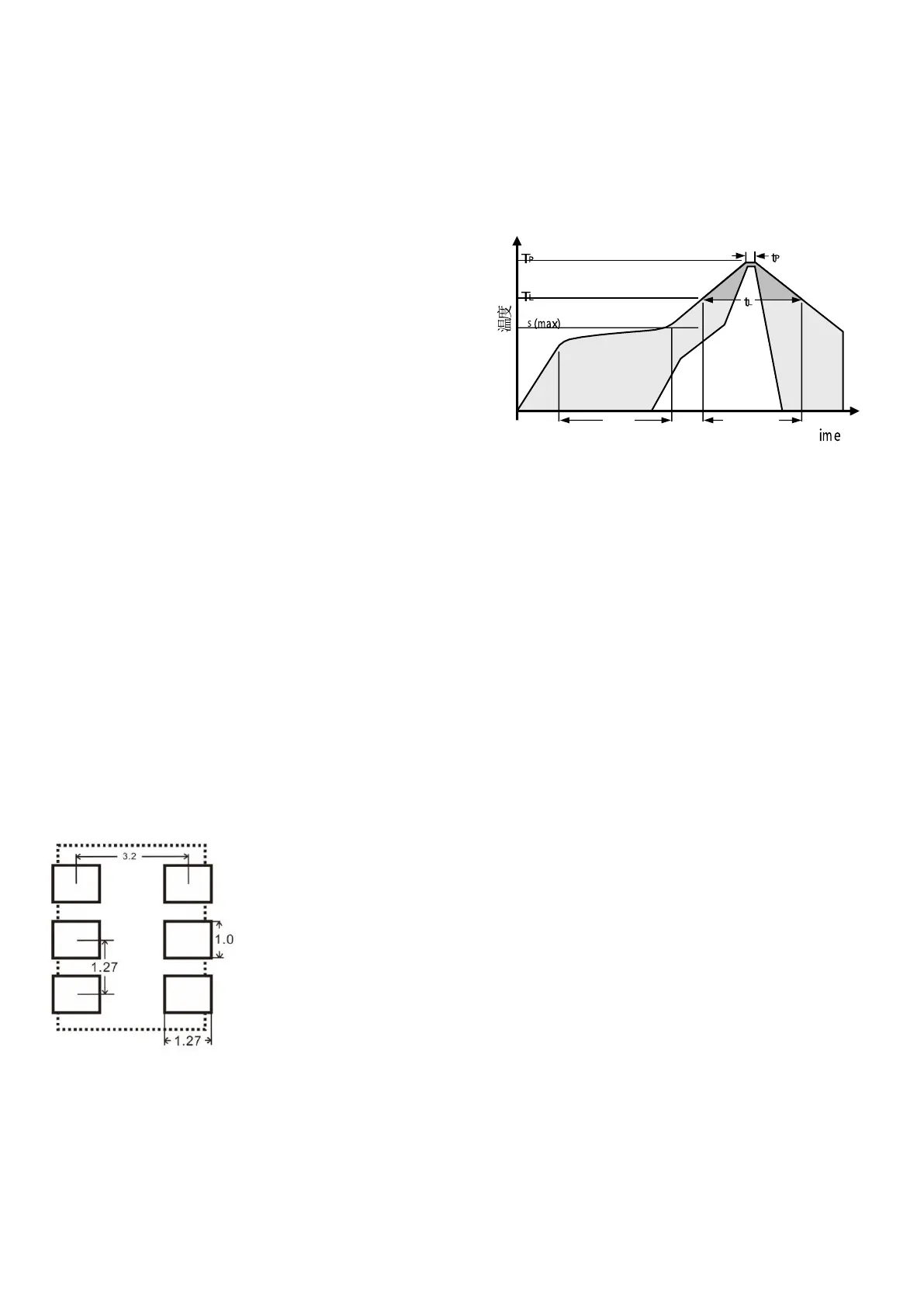
Figure 9 JEDEC standard welding process diagram, Tp <= 260 ° C, tp < 30 sec ,
lead-free soldering Pick up. TL<220°C, tl<150sec , the rate of temperature rise
and fall during welding Should be <5 ° C / sec .
The AHT10 can be soldered using a standard reflow
oven . The sensor is fully compliant with the IPC/JEDEC
J-STD-020D soldering standard. The contact time
should be less than 40 seconds at temperatures up to
260 °C ( see Figure 9) ; the ultimate soldering
temperature that the sensor can withstand is 260 °C .
Note: After reflow soldering, the sensor should be
stored in a >75% RH environment for at least 12 hours
to ensure rehydration of the polymer. Failure to do so
will cause the sensor reading to drift. It is also possible
to place the sensor in a natural environment ( >40%
RH ) for more than 5 days to rehydrate it. Use low
temperature reflow soldering
(Example : 180 ° C) can reduce hydration time.
Do not flush the board after soldering. Therefore, customers are advised
to use " no-clean " solder paste. If the sensor is used in corrosive gases
or if condensed water is produced (eg, in a high-humidity environment),
both the lead pad and the PCB need to be sealed (eg, using a conformal
coating) to avoid poor contact or short circuit.
 Loading...