4.2 Input / output characteristics
Electrical characteristics, such as power
consumption, high and low voltages of the input
and output, etc., depend on the power supply
voltage. In order to make the sensor
communication smooth, it is important to ensure
that the signal design is strictly limited to the ranges
given in Tables 7 , 8, and 12 .
VDD = 3.3V,
-4mA< IOL<
0mA
VDD = 3.6 V,
VIN=0Vto3.6V
Table 7 DC characteristics of the digital input and output pads, if there is no
special statement, VDD = 1.8 V to 3.6 V, T = -40 ° C to 85 °C.
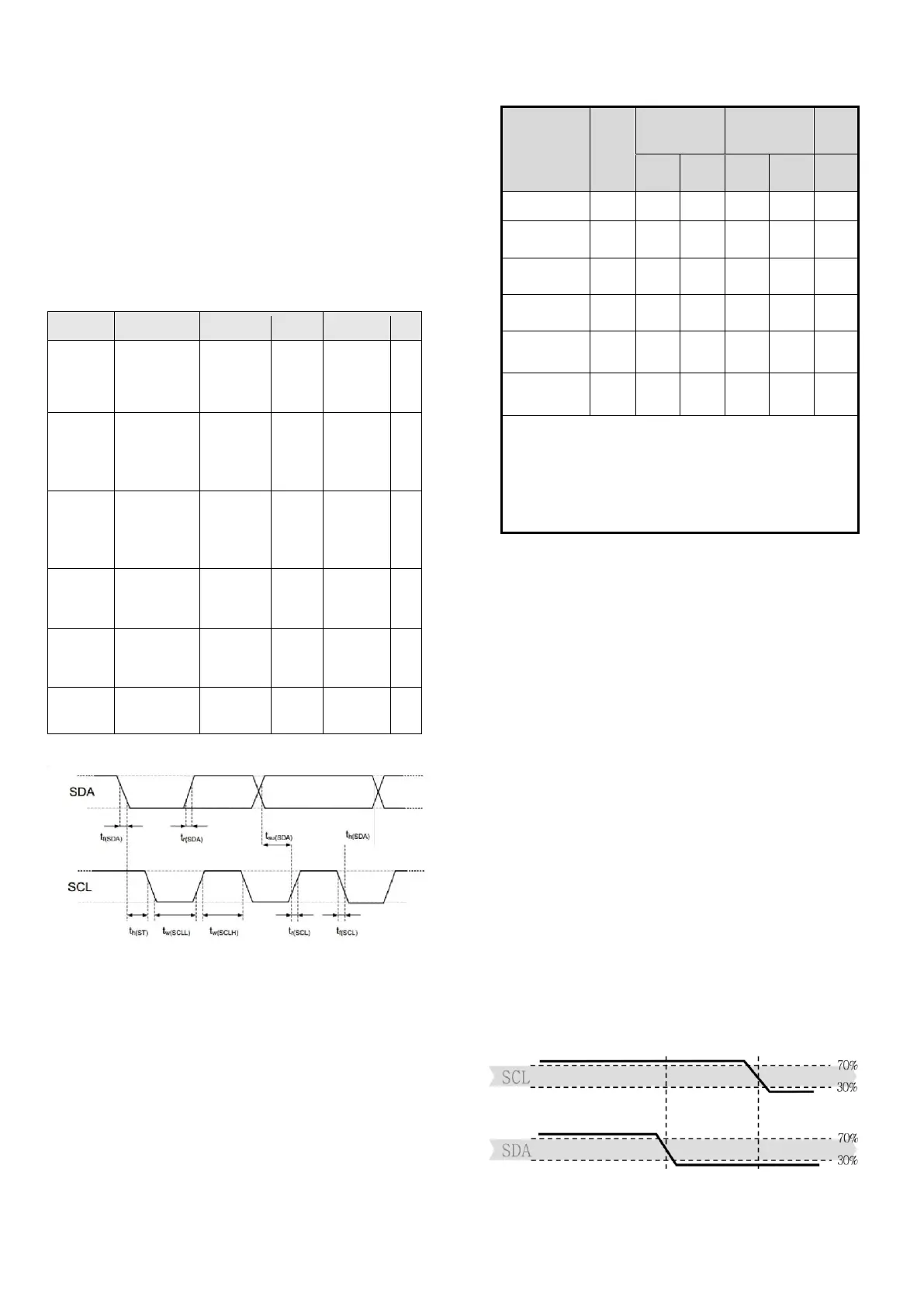
Figure 12 shows the timing diagram and abbreviations of the digital input
/ output terminals in Table 8 .
Explanation. The thicker SDA line is controlled by the sensor, the normal
SDA line
Controlled by a single chip microcomputer. Please note that the effective
read time of SDA is from the previous one.
Triggered by the falling edge of the conversion.
SCL clock high
level width
Data retention
time relative to the
SCL SDA edge
Data setup time
relative to the SCL
SDA edge
Note : Measurements for both pins are from 0.2VDDand0.8VDD.
Note : The above I 2 C timing is determined by the following internal
delay:
(1) The internal SDI input pin is delayed relative to the SCK pin,
typically 100ns
(2) The internal SDI output pin is delayed relative to the SCK falling
edge, typically 200ns
Table 8 Timing characteristics of the I2C fast mode digital input / output.
The specific meaning is shown in Figure 12. Unless otherwise stated.
5 Sensor communication
The AHT10 communicates using the standard I 2 C
protocol. For information on the I 2 C protocol other
than the following sections, please refer to the
following website : www.aosong.com provides a
sample program reference.
5.1 Start sensor
The first step is to power up the sensor and the
voltage is selected. VDD supply voltage (range
between 1.8V and 3.6V). After power-on, the sensor
needs at most 20 milliseconds time SCL is high) to
reach the idle state, ready to receive commands sent
by the host (MCU).
5.2 Start / stop timing
Each transmission sequence is The Start state is
started and ends with the Stop state, as shown in the
figure. 13 and map 14
 Loading...