深圳市博安通科技股份有限公司 中山市博安通通信技术有限公司
SHENZHEN B&T TECHNOLOGY Co., Ltd ZHONGSHAN B&T TECHNOLOGYCo., Ltd
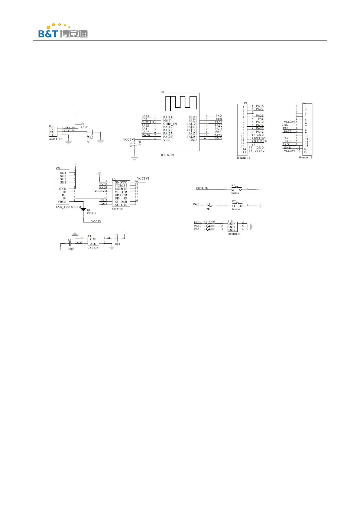
5.Schematic diagram
6.Design guidance
Power supply
The development board supports 3.3V or 5V voltage with peak current above 500mA
GPIO port
Some GPIO ports are lead out from the periphery of the module, if using the proposed resistance
of 10-100 ohms in series on the corresponding IO port. That can suppress the overshoot,
smoother on both sides.Help for both EMI and ESD.
The up and down of the special IO port, refer to the specification instructions, which affects the
start up configuration of the module.