UDAC
11
5
O Video DAC output.
F: CVBS/chroma signal for simultaneous mode
.
Y:
Luma component for YUV and Y/C processing.
C: Chrominance signal for Y/C processing.
U: Chrominance component signal for YUV mode
.
V: Chrominance component signal for YUV mode.
YUV0 O YUV pixel 0 output data
.
PIXOUT0 O CCIR656 output pixel 0.
TW
S
11
6
O Audio transmit frame sync output.
SEL_PLL2 I System and DSCK output clock frequency selection is
made at the rising edge of
RESET#. The matrix below lists the available clock frequencies and their
respective PLL bit settings.
Strapped to VCC or ground via 4.7-k&! resistor; read-
only during reset.
ES6688A Pi
n Description (Continued)
Names Pin Numbers I/
O Definitions
Value
F DAC
(pin 109)
V DAC
(pin 110)
Y DAC
(pin
1130
C DAC
(pin 114)
U DAC
(pin 115)
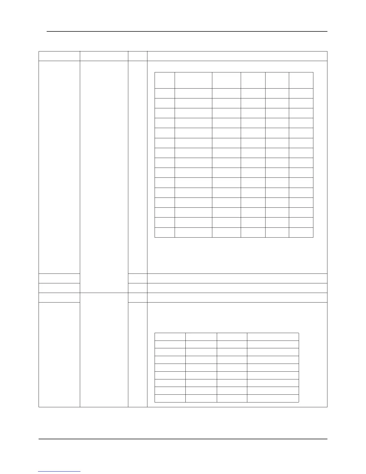
0 CVBS/Chroma CVBS1 Y C N/A
1 CVBS/Chroma CVBS1 Y C CVBS2
2 CVBS/Chroma N/A Y C N/A
3 CVBS/Chroma CVBS1 N/A N/A CVBS2
4 CVBS/Chroma CVBS1 N/A N/A N/A
5 CVBS/Chroma CVBS1 Y Pb Pr
6 CVBS/Chroma N/A Y Pb Pr
7 N/A
SYNC G B R
8 CVBS/Chroma Chroma Y Pb Pr
9 CVBS CVBS1 G B R
10 CVBS CVBS1 G R B
11 N/A SYNC G R B
12 CVBS/Chroma N/A Y Pr Pb
13 CVBS/Chroma
CVBS1 Y Pr Pb
14 Chroma Y G R B
SEL_PLL2 SEL_PLL1 SEL_PLL0 Clock Type (MHz)
0 0 0 CLK
⋅ 4.5
0 0 1 CLK ⋅ 5.0
0 1 0 Bypas
s
0 1 1 CLK
⋅ 4.0
1 0 0 CLK
⋅ 4.25
1 0 1 CLK
⋅ 4.75
1 1 0 CLK
⋅ 5.5
1 1 1 CLK
⋅ 6.0