BG0836 1/2.7 inch 1080P HD CMOS image sensor
16/ 24
PLL control
pre-divider
pln_p<5:0>
clkin
PFD
CP
LPF
VCO
vco_fsel_p<1:0>
loop-divider
plm_p<8:0>
pllclk_sel
clkin
fvco
fvco
pln_p+2
plm_p+2
pclk_sel
pclkdiv<2:0>
fpll=fvco
fpll
pclkdiv+2
pixclk
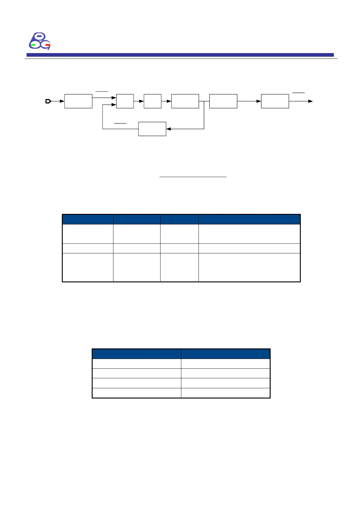
Figure 12 PLL block diagram
The relationship between output Pclk frequency and clkin frequency is :
Registers corresponding to PLL are listed in Table 10:
Table 10 PLL control register
Bit[6] Reserved
Bit[5:4] vco_freq_sel
Bit[2:0] pclkdiv
When you adjust vco oscillation frequency, you need to set vco_freq_sel of PLLCTRL_P. Formula
for vco frequency is
Setting vco_freq_sel according to the following table.
Table 11 PLL VCO frequency setting up corresponding table
Main System Clock control
Mclk(Main System Clock)can be chosen as Clkin (external clock ) or the frequency
multiplication of Pclk(Pixel output clock).



 To Next Page