EasyManua.ls Logo

Cambridge Audio Azur 540A V2.0 User Manual

Cambridge Audio Azur 540A V2.0
42 pages
To Next Page IconTo Next Page
Page #1 background imageLoading...
Page #1 background image
Gallery Court Hankey Place London SE1 4BB UK
Tel: +44 (0)20 7940 2200 Fax: +44 (0)20 7940 2233
540A V2
Issue Date: 31
st
March 2006
_________________________________________________________________________________________
SERVICE MANUAL
_________________________________________________________________________________________
SPECIFICATIONS:
Power Output 60W (into 8)
90W (into 4)
THD (unweighted) <0.002% @ 1kHz, of rated power
<0.070% 20Hz – 20kHz, of rated power
<0.025% 20Hz 20kHz @ 10w
Frequency response (-1dB) 5Hz – 50kHz
S/N ratio (ref 1w) >85dB
Input impedances 47kohms
Power Amp damping factor >100
Max power consumption 650w
Min/On power consumption <35w (no signal)
Standby power consumption <10w
Bass / Treble controls Shelving, ultimate boost/cut + /-7.5dB
@ 20Hz and 20kHz
Dimensions 100 x 430 x 310mm
(3.9 x 16.9 x 12.2”)
Weight 7.4kg (16.3Lbs)
AP19973/1
1
Question and Answer IconNeed help?

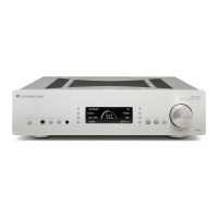
Do you have a question about the Cambridge Audio Azur 540A V2.0 and is the answer not in the manual?

Cambridge Audio Azur 540A V2.0 Specifications

General IconGeneral
Input Impedance47 kOhms
Input Sensitivity200 mV
Damping Factor> 100
Dimensions430 x 100 x 320 mm
Power Output60W per channel (8 Ohms)
Total Harmonic Distortion (THD)<0.01% (1kHz, 50W)
Signal-to-Noise Ratio>90dB

Summary

General Information and Safety

Specifications

Technical performance details and operational parameters of the 540A V2 amplifier.

Safety Precautions & Important Notes

Essential safety guidelines for operating and servicing the Cambridge Audio 540A V2 amplifier.

Exploded Diagram

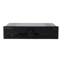
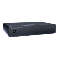
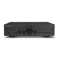
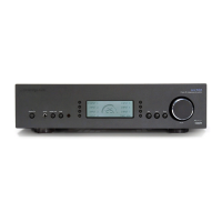
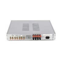
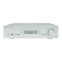
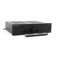
Visual representation of the amplifier's components for identification and assembly.

Input PCB Documentation

Input PCB Schematics

Circuit diagrams for various sections of the input PCB.

Input PCB Layouts

Physical layouts of the input PCB's top and bottom sides.

Input PCB Assembly BOM

Bill of Materials for the input PCB assembly.

Voltage Select Switch Documentation

Voltage Select Switch Schematic

Circuit diagram for the voltage selection switch.

Voltage Select Switch Layouts

Physical layouts of the voltage select switch PCB's sides.

Voltage Selector PCB BOM

Bill of Materials for the voltage selector PCB.

Mains and Front Panel PCB Documentation

Mains PCB Schematic

Circuit diagram for the mains power input section.

Front Panel PCB Schematic

Circuit diagram for the front panel interface and controls.

Front Panel & Mains PCB Layouts

Physical layouts of the front panel & mains PCB's sides.

Front Panel and Mains PCB Assembly BOM

Bill of Materials for the front panel and mains PCBs.

Amplifier PCB Documentation

Amp PCB Schematics

Circuit diagrams for amplifier stages and protection.

Amp PCB Layouts

Physical layouts of the amplifier PCB's top and bottom sides.

Amp PCB Assembly BOM

Bill of Materials for the amplifier PCB assembly.

Abus Module Documentation

Abus Module Schematic

Circuit diagram for the Abus module.

Abus Module Layouts

Physical layouts of the Abus module PCB's sides.

A-Bus PCB BOM

Bill of Materials for the A-Bus PCB.

Component Pin Layouts

IC Pin Layout Details

Pin configurations and diagrams for various integrated circuits.

Related product manuals