Diodes D12 and D13 provide short circuit protection. With an improper load con
-
nected to the OUTPUT, the voltage drop across R71 and R72 forward bias diodes D12
and D13 respectively. For this condition, the respective OUTPUT transistor is by
-
passed, the OUTPUT current is derived from the op-amp and limited to approximately
± 200 mA. Diodes D9 and D10 provide limiting preventing OUTPUT transistors satu
-
ration which prohibits base-emitter charge storage, enhancing good overload recover.
Two AMP OUTPUTS are provided. The front panel OUTPUT provides either ≤ 1
ohm or 93 ohm OUTPUT impedance, drive up to 10 feet of 93 ohm coax cable where
the 93 ohm OUTPUT can drive a few hundred feet. The rear panel has a fixed 93 ohm
series-connected OUTPUT impedance.
Restorer
The restorer circuitry consists of OUTPUT amplifier A3, transistor array Al, a dual
differential comparator A2 and transistors Q4 through Q7, Q29 and Q30. The restorer
is a transconductance type amplifier that is; it monitors the AMP OUTPUT (TP1)
OUTPUT voltage and develops a constant current of correct polarity at its OUTPUT
(junction of Q4 collector and A1e pin 15). The voltage on C24 is buffered by FET Q6
and summed in at A3 pin 3, forcing the AMP OUTPUT (TP1) to 0 volts maintaining
the baseline. The AMP OUTPUT signal (TP1) is clamped by diode network D15 and
D16 and connected to the comparator input A2 pins 5 and 2. If A2 detects a signal, its
OUTPUT turns Q29 off. Q7 switches on a current sufficient to back bias current
source A1a disabling the restorer. Capacitor C40 ac couples the transistor Q29 pre-
venting potential restorer latch up problems.
The negative restorer gate threshold is set at –100 mV by resistors R103 and R100.
The positive threshold is variable and depends on the coarse gain switch setting S1a
(section R2), and resistors R94 through R99. Pot RV3 adjusts the restorer offset and
AMP OUTPUT (TP1) to 0 ± 5 mV dc.
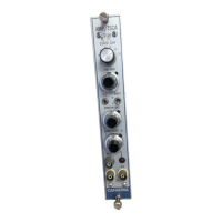
SCA Section
SCA OUTPUT
In the following discussion, Logic “l” is referred to as a high voltage level of +2.4 to
+5 volts. A Logic “0” is referred to as a low voltage level of 0 to +0.8 volts.
33
SCA Section