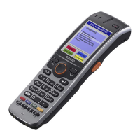
— 55 —
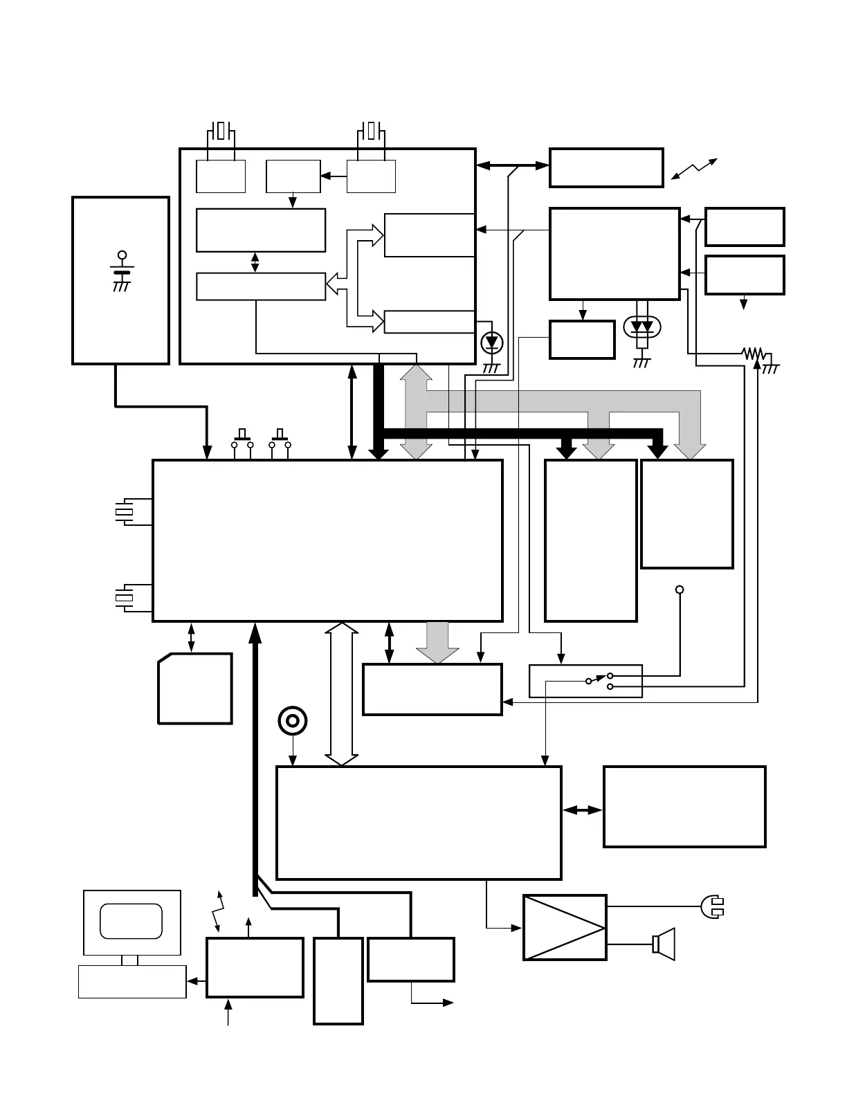
10. CIRCUIT BLOCK DIAGRAM
Timer clock
32.768kHz
CPU
OSB
VR4122
KEYS
CORE of CPU
* Power supply
* Voltage regulator
LED IF
45.158MHz
DRAM x 2
ROM x 2
DRAM1/ DRAM2
32 Mbytes
(16 Mbytesx2)
Fast IrDA clock
Back light
* Touch Panel IF
* Voltage detection
AC Adapter
* Charge control
AD-C59200
(To Cradle)
DC/AC
Inverter
V5LCD
DATA BUS
RESET
POWER ON/OFF
ADDRESS BUS
System clock
GATE ARRAY (ASIC): KUJIRA
*KUJIRA is a Japanese nickname for this Gate Array, and
can not be replaced as well as above CPU because of BGA
* For Communication and LCD drive/control etc.
48MHz
Voltage
LCD (TFT) Module
VCOM
CF/MODEM
Card
(US and
Canada only)
Battery power detection
IC300
Touch Panel
* Battery Power detection
* HP/ SP drive
Headphone
IC401
CRADLE
PC
To Analog Telephone line
(From AC adapter)
System clock for CPU
18.432MHz
150MHz
IC700
IrDA Module
IC2
(BGA)
OSBPLL
General Purpose
Interface
IC200
Rechargeable
Battery
Power IC
Charge LED
Alarm LED
(RED)
(Amber/ Green)
Bus Control Unit
(Key PCB)
IC 1
IC1/IC2
16 Mbytes
(8 Mbytesx2)
VSUB
IC303
240 x 320 dots
MIC
Speaker
MODEM
(US & Canada
only)
Phone
Mobile
Power supply
Action/ Voice etc.
VSUB
Instruction/ Cache Mem.
CRADLE
IrDA
Mpdule
 Loading...