– 14 –
6. PIN FUNCTION
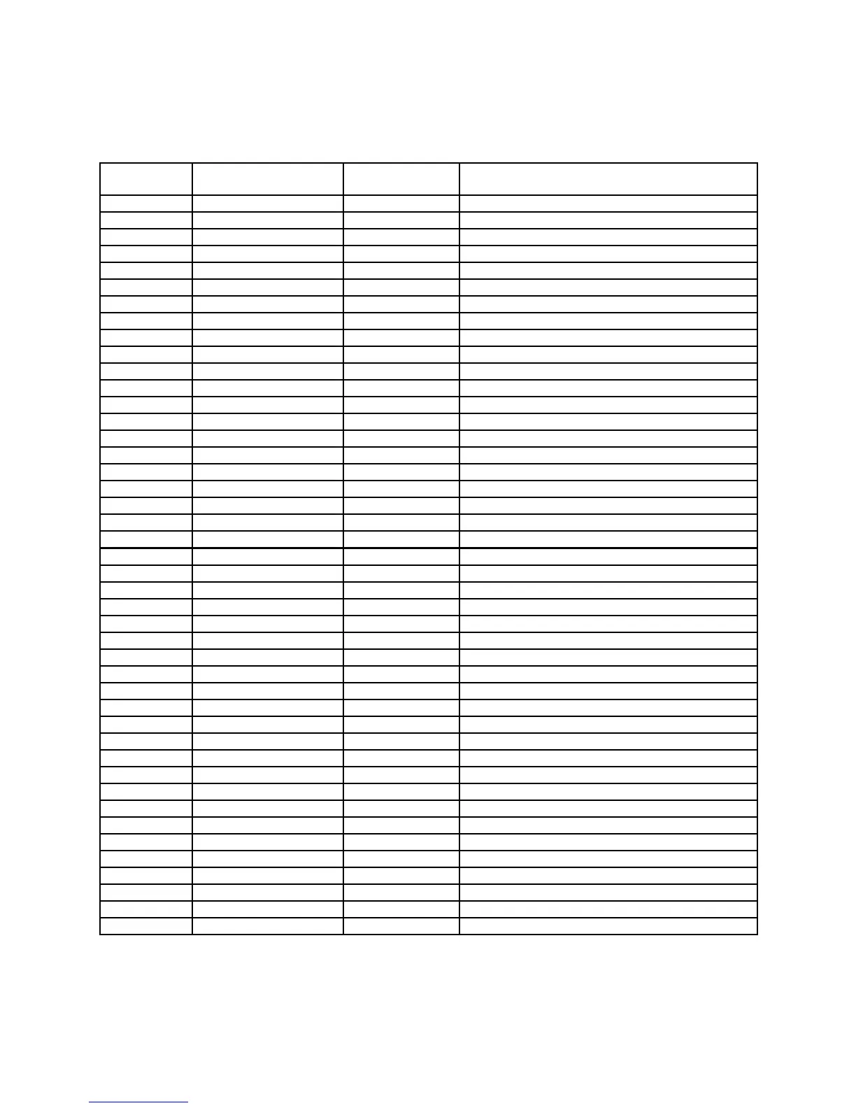
CPU (HWD62096A03)
Pin No. Pin Name Input / Output Function
1 VSS Power supply for LSI, GND
2 VREG5 Regulator power, +5V
3 VREG4 Regulator power for ROM, +3V
4 VREG2 Regulator power, +2V
5 VDT1I I Terminal for detector (All off)
6 VDT2A O Terminal for detector (Lower battery)
7 VDT2b I Terminal for detector (Lower battery)
8 VREG1 Regulator power, +3.2V
9 VREG3 Regulator power for RAM, +3V
10 VCC Power supply for LSI, +6V
11,12 TS1,TS2 I Terminal for test
13 SW I Reset switch
14~25 KO1~KO12 O Terminal for key output
26~33 KI1~KI8 I Terminal for key input
34 ITO I Terminal for interrupt
35 RXD I Terminal for communication
36 TXD O Terminal for communication
37 OPTO O Output terminal
38 BUFON O Output terminal
39~50 AO6~AO17 O Address bus
51 VSS Power supply for LSI, GND
52,53 BZZ1,BZZ2 O Terminal for buzzer
54 VSS Power supply for LSI, GND
55~60 AO0~AO5 O Address bus
61 OEBO O Output enable terminal
62 WEBO O Write enable terminal
63~69 CS4BO~CS10BO O Chip selecter terminal
70~77 IO0~IO7 I/O Data bus
78~85 PORT0~PORT7 I/O Input/output port
86 DUMMY Dummy terminal
87,88 PI,PO Power for ceramic oscillator
89 VSSL Power supply for LSI, GND
90,91 XO,XI Power
92 DUMMY Dummy terminal
93 VSSR Power supply for LSI, GND
94~221 S1~S128 O Terminal for LCD
222~285 C1~C64 O Terminal for LCD
286 DUMMY Dummy terminal
287 VLCD Power supply for LCD, +12V
288~291 V1~V4 Power supply for LCD bias
292~296 VOL0~VOL4 Power supply for LCD contrast
297 DUMMY Dummy terminal
298~301 VD1~VD4 Power for doubler
302 VDB Power for doubler, +12V
 Loading...