— 15 —
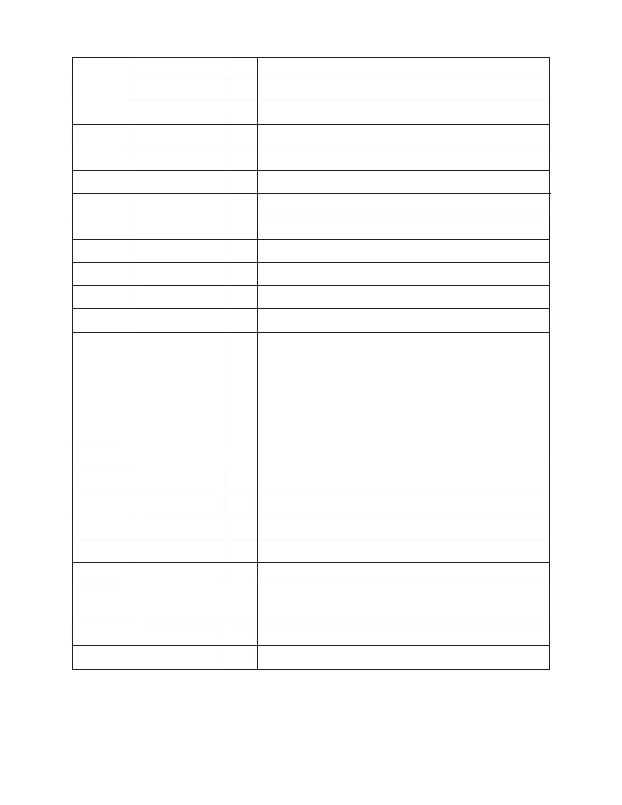
Pin No. Signal In/Out Function
75 ~ 77 PORT4 ~ 6 In/Out For data communication
78, 79 PORT2, 3 – Interrupt port
80 PORT1 In Communication data through Photo Sensor
81, 82 – Not used
83, 84 PI, PO In/Out Main clock terminal (3.45 MG)
85 DUMMY – Not used
86, 87 XI, XO In/Out Clock terminal (DT-26S)
88 DUMMY – Not used
89 ~ 184 S1 ~ 96 Out Segment signal for display
185 ~ 216 C1 ~ 32 Out Common signal for display
217 VSSR In GND / 0[V]
218 ~ 222 V0 ~ 4 Out The voltage for LCD drive
OFF : 0[V]
ON; V0 : 3.6 (Min) ~ 5.8 (Max) [V]
V1 : 2.9 (Min) ~ 4.6 (Max) [V]
V2 : 2.1 (Min) ~ 3.5 (Max) [V]
V3 : 1.4 (Min) ~ 2.4 (Max) [V]
V4 : 0.7 (Min) ~ 1.2 (Max) [V]
223, 224 VSS In GND / 0[V]
225 DUMMY – Not used
226 VCC In Power supply / 3[V]
227 VREG2 Out 2 [V]
228, 229 TS1, 2 – Test for manufacturer
230, 231 BZ1, 2 Out Buzzer terminal
232 SW1 In 2.6[V]
While pushing the reset button: 0[V]
233, 234 VD1, 2 – VD1: 4.7[V] VD2: 1.6[V]
235, 236 VD3, 4 – VD3: 4.7[V] VD4: 1.6[V]