— 14 —
6. LSI PIN FUNCTION
1. CPU (HC3000-08-F1)
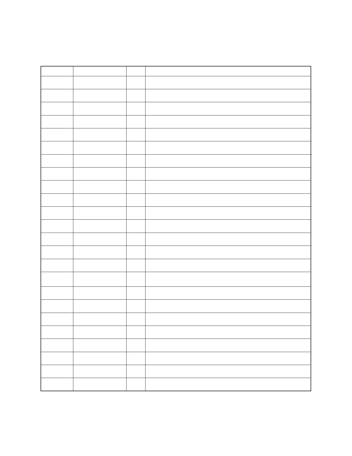
Pin No. Signal In/Out Function
1 VREG3 Out Power supply for RAM / 3(V)
2 DUMMY – Not used
3 ~ 5 KO10 ~ 12 Out Not used
6 ~ 14 KO1 ~ 9 Out Key scan signal
15 KI8 In Not used
16 ~ 22 KI1 ~ 7 In Key input signal
23 , 25 TRANS, DUMMY – Not used
24 BUFON Out Power supply control for ROM
26 IT2 In Interrupt signal input
27 IT0 In Reception data input
28 AO17 Out Not used
29 ~ 45 AO0 ~ 16 Out Address bus
46 OEB0 Out Output enable signal for RAM and ROM
47 WEB0 Out Write enable signal for RAM
48 ~ 52 – Not used
53 CS7B0 Out Chip enable signal for RAM
54 CS6B0 Out Chip enable signal for ROM
55, 56 Out Not used
57 ~ 64 IO0 ~ 7 In/Out Data bus
65, 66 – Not used
67 OPT6 Out Turn on signal for Photo Sensor
68, 72 OPT1, 5 Out Turn on signal for LED (Infrared)
69 ~ 73 – Not used
74 PORT7 – Interrupt port