Pin No. Terminal In/Out Function
1, 2 TEST1, TEST2
—
Not used. Connected to ground.
3 RESET In Power ON reset terminal. On: +5 V Off: 0 V
4 AVDD In +5 V source for the built-in DAC
5 OUT Out Sound waveform output
6 AGND In Ground (0 V) source for the built-in DAC
7 GND In Ground (0 V) source
8 COSI In 21.725 MHz clock pulse input
9 COSO
—
Not used
10 VDD In +5 V source
11 ~ 18 KI0 ~ KI7 In Input terminals from keys and switches
19, 20 KO11, KO10
—
Not used
21 ~ 30 KO9 ~ KO0 Out Key and switch scan signal outputs
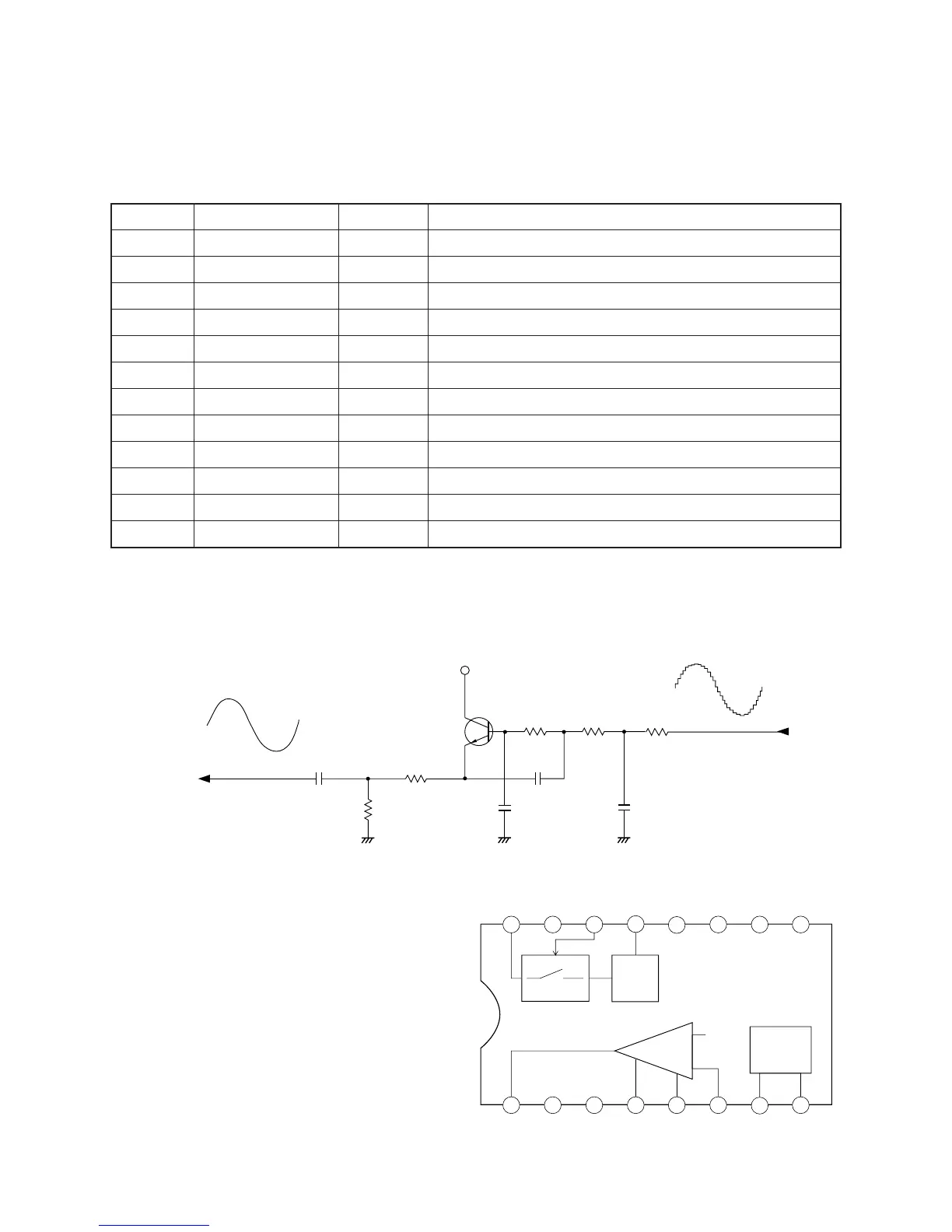
CPU (LSI101: MSM6387-13)
Containing a sound data ROM and a DAC (Digital to Analog Convertor), the CPU provides sound waveform
in accodance with the pressed key and the selected tone.
The following table shows the pin functions of LSI101.
Filter Block
Since the sound signal from the CPU is a stepped waveform, the filter block is added to smooth the waveform.
AVDD
C108
Q101
2SC1740SQ
C107
AG
R107
R2106
C106
C109
AG
R105
AG
R104
R108
To power amp
From CPU
Amplifier/Voltage Regulator
(IC101: AN8053N)
The right figure shows the internal block of IC101.
16
15
14 13
12 11
10
9
8
7
6
5
4
32
1
SP AMP
VREF
5V REG
POWER
SPO NC SP GND PC-1 PC-2 SPI SPM VREF
VCC NC CONT
5V
VREG
NCNC NC PRE GND
+
-
— 4 —