Schematic Diagrams
B-1
B.Schematic Diagrams
Appendix B: Schematic Diagrams
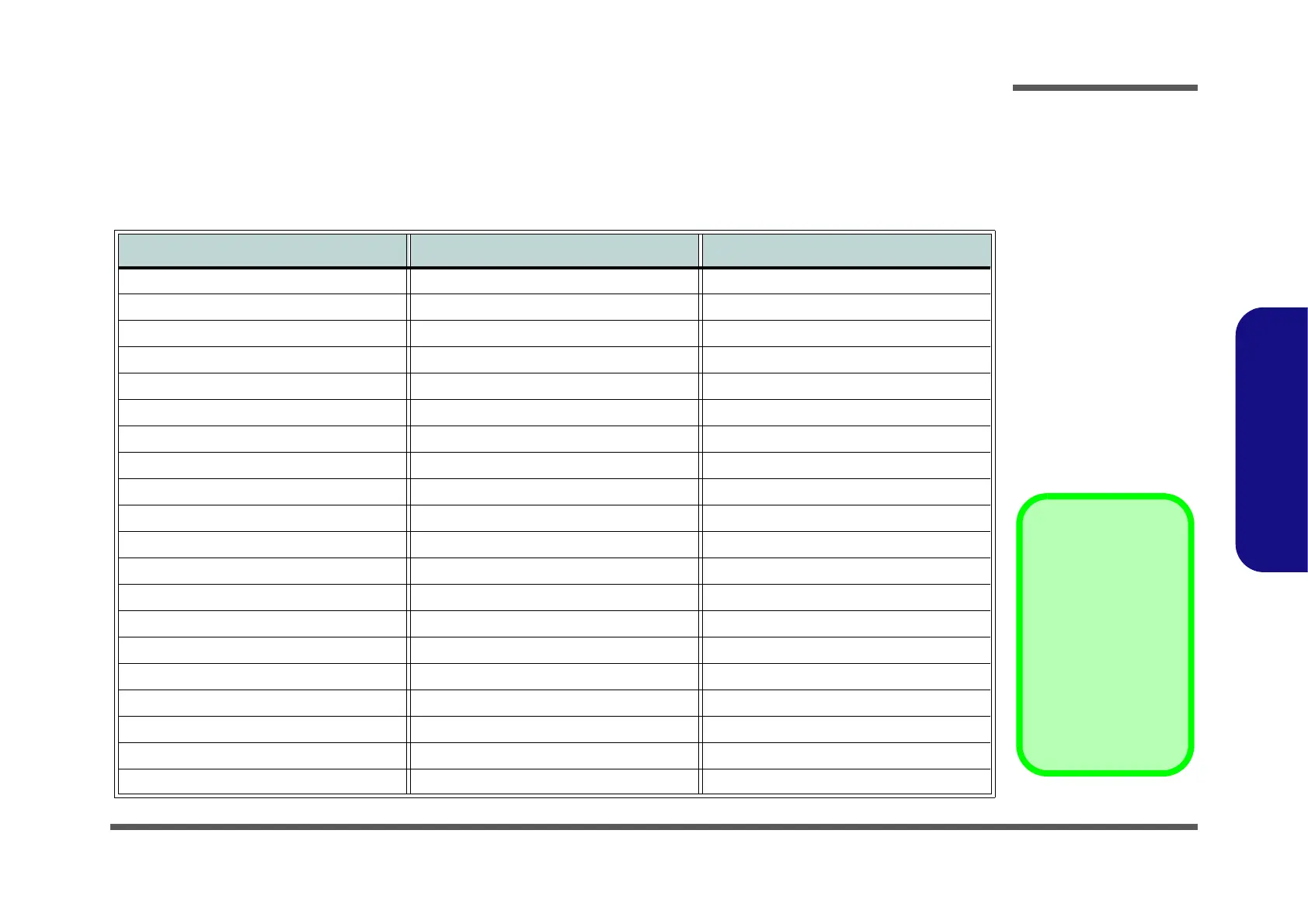
This appendix has circuit diagrams of the W370SS notebook’s PCB’s. The following table indicates where to find the
appropriate schematic diagram.
Diagram - Page Diagram - Page Diagram - Page
System Block Diagram - Page B - 2 VGA NVVDD Decoupling - Page B - 22 VDD3, VDD5 - Page B - 42
Haswell 1/7 - Page B - 3 Lynx 1/9 - Page B - 23 1.5V or 1.35V / 0.75VS, 1.5VS - Page B - 43
Haswell 2/7 - Page B - 4 Lynx 2/9 - Page B - 24 1.05VS, 1.05V_M, 1.05V_LAN_M - Page B - 44
Haswell 3/7 - Page B - 5 Lynx 3/9 - Page B - 25 Power V-Core - Page B - 45
Haswell 4/7 - Page B - 6 Lynx 4/9 - Page B - 26 VGA NVVDD, PEX_VDD - Page B - 46
Haswell 5/7 - Page B - 7 Lynx 5/9 - Page B - 27 FBVDDQ - Page B - 47
Haswell 6/7 - Page B - 8 Lynx 6/9 - Page B - 28 AC-In, Charger - Page B - 48
Haswell 7/7 - Page B - 9 Lynx 7/9 - Page B - 29 W370SS/W350SSQ Audio Board - Page B - 49
DDR SO-DIMM A_0 - Page B - 10 Lynx 8/9 - Page B - 30 W370SS/W35XSSQ Power LED Board - Page B -
DDR SO-DIMM B_0 - Page B - 11 Lynx 9/9 - Page B - 31 W370SS/W35XSSQ Click Board - Page B - 51
DDR SO-DIMM A_1 - Page B - 12 Mini PCIE, Fan, Audio Con - Page B - 32 W370SS Power Switch Board - Page B - 52
PS8625 - Page B - 13 USB Charge, CCD, TPM, Multi-Con - Page B - 33 W350SSQ Power Switch Board - Page B - 53
Panel, Inverter, CRT - Page B - 14 ESATA/USB3.0 Connector - Page B - 34 W370SS LID / VGA LED Board - Page B - 54
VGA PCI-E Interface - Page B - 15 Card Reader / LAN RTL8411B - Page B - 35 W35XSSQ LID / VGA LED Board - Page B - 55
VGA Frame Buffer Interface - Page B - 16 SATA HDD, VLED CON, LID SW - Page B - 36 W350SSQ VGA / WLAN SW Board - Page B - 56
VGA Frame Buffer A - Page B - 17 HDMI, RJ45 - Page B - 37 W355SSQ Power Switch Board - Page B - 57
VGA Frame Buffer A - Page B - 18 Audio Codec VT1802S - Page B - 38 W355SSQ VGA / WLAN SW Board - Page B - 58
VGA Frame Buffer B - Page B - 19 Audio AMP & Con - Page B - 39 POWER SEQUENCE - Page B - 59
VGA Frame Buffer B - Page B - 20 KBC ITE IT8587 - Page B - 40
VGA I/O - Page B - 21 5V, 5VS, 3.3V, 3VS, 3.3VM - Page B - 41
Table B - 1
Schematic
Diagrams
Version Note
The schematic dia-
grams in this chapter
are based upon ver-
sion 6-7P-W355B-001.
If your mainboard (or
other boards) are a lat-
er version, please
check with the Service
Center for updated di-
agrams (if required).
 Loading...