D D
C C
B B
A A
M/B USB port0 (2.0+3.0)
M/B USB port1 (2.0+3.0)
M/B USB port0 (2.0+3.0)
M/B USB port1 (2.0+3.0)
CCD
BLUETOOTH
A/B USB port3 (2.0)
AMI Debug Use
When the platform does not use the
USB2_OTG_ID and USB2_VBUS_SNS pins,
USB2_OTG_ID pin should be unconnected on
the platform (terminated with internal
pull ups] and USB2_VBUS_SNS should be
connected to ground.
Internal PD 20K CMOS
Internal PD 20K CMOS
Enable CSE ROM Bypass
0=disable bypass (default)
1=enable bypass
Force DNX FW Load
0=do not force (default)
1=Force
Internal PD 20K CMOS
TC_CLK_TIMER_BYPASS
0=not bypassed (default)
1=bypassed
Internal PD 20K CMOS
Internal PU 20K CMOS
Allow eMMC as a boot source
0=do not allow
1=allow
Internal PU 20K CMOS
Allow SPI as a boot source
0=do not allow
1=allow
Hardware Straps (3)
Internal PU 20K CMOS
LPC Boot BIOS
0=don't boot from LPC (default)
1=boot from LPC
2016/5/30
pull high/low strap wrong
2016/6/15
delete R27, R282, R283, R284, R285, R286, R287, R288, Q16, T34, T35
2016/6/15
add R282, R283, T34
3G + LTE
A/B USB port2 (2.0)
3G + LTE
W97 CARD READER
2016/6/22
3G/LTE change to USB port-2
2016/6/22
W97 CARD READER change to PCIE port-4
2016/6/22
3G/LTE change to USB port-2
2016/6/22
A/B USB port2 change to USB port-3
2016/8/15
delete net EMMC_RST#
SOC_GPIO219
UART1_RXD
UART2_RXD
SOC_GPIO47
SOC_GPIO40
SOC_GPIO39
USB_OC1#
USB_OC0#
USB_VBUSSNS
USB_RCOMP
SSIC_RCOMP
SOC_GPIO49
USB_OTG_ID
SOC_GPIO44
SOC_GPIO43
SOC_GPIO49
SOC_GPIO47
SOC_GPIO48
SOC_GPIO39
SOC_GPIO40
SOC_GPIO43
SOC_GPIO44
SOC_GPIO48
PCIE_TXP4_C
PCIE_TXN4_C
1.8VA
1.8VA
1.8VA
USB_PP619
USB_PN619
USB_PP721
USB_PN721
USB_PN0 22
USB_PP0 22
USB_PN1 22
USB_PP1 22
USB_PP4 19
USB_PN4 19
USB3_RX0_P22
USB3_RX0_N22
USB3_TX0_N22
USB3_TX0_P22
USB3_RX1_P22
USB3_RX1_N22
USB3_TX1_N22
USB3_TX1_P22
SMI# 23
USB_PN2 21
USB_PP2 21
USB_PP3 19
USB_PN3 19
USB3_RX2_P21
USB3_RX2_N21
USB3_TX2_N21
USB3_TX2_P21
PCIE_TXP4_CARD18
PCIE_TXN4_CARD18
PCIE_RXP4_CARD18
PCIE_RXN4_CARD18
Title
Size Document Number R e v
Date: Sheet
of
1.0
[06] APL SOC_5/8_USB,GPIO
A3
6
33Tuesday, November 15, 2016
ᙔ!Ϻ!ႝ!တ!!DMFWP!DP/
W940PU_D02
6-71-W94P0-D02
Title
Size Document Number R e v
Date: Sheet
of
1.0
[06] APL SOC_5/8_USB,GPIO
A3
6
33Tuesday, November 15, 2016
ᙔ!Ϻ!ႝ!တ!!DMFWP!DP/
W940PU_D02
6-71-W94P0-D02
Title
Size Document Number R e v
Date: Sheet
of
1.0
[06] APL SOC_5/8_USB,GPIO
A3
6
33Tuesday, November 15, 2016
ᙔ!Ϻ!ႝ!တ!!DMFWP!DP/
W940PU_D02
6-71-W94P0-D02
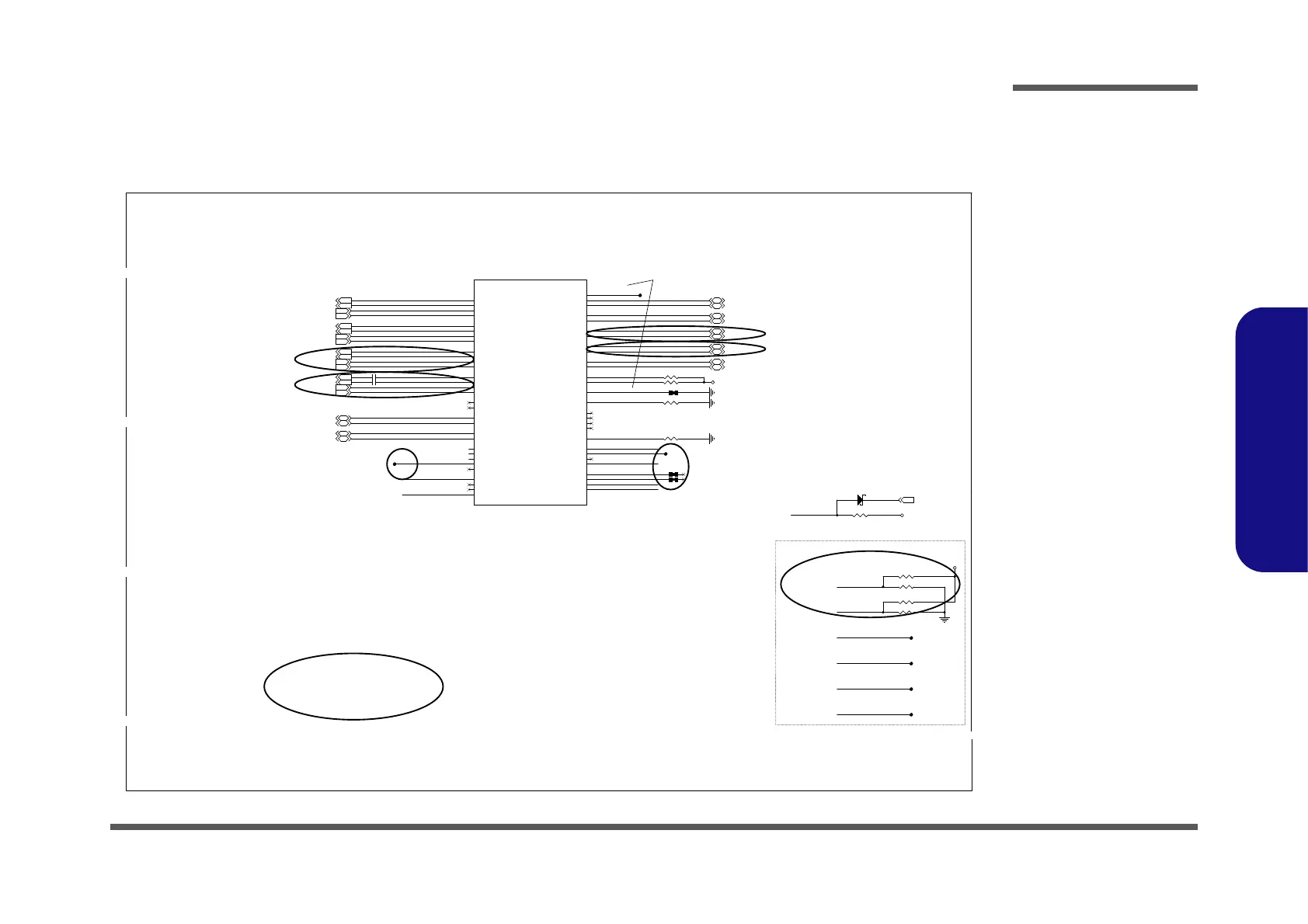
APL_SOC
USB3.0
USB2.0
HSIC
UART
U1F
USB3_TXP1
K3
USB_DN2
V13
USB_DN3
V7
USB_RCOMP
Y15
GPIO43/UART1_TXD
B43
GPIO42/UART1_RXD
C43
GPIO45/UART1_CTS_B
C42
GPIO44/UART1_RTS_B
A42
USB3_TXP0
J1
USB_DP4
Y9
USB_DN0
V10
USB_DN1
V15
USB_VBUSSNS
AC16
USB_OTG_ID
AC15
USB3_TXN0
J2
USB3_TXN1
K2
PCIE_TXP5/USB3_TXP2
L2
USB_DN4
Y10
USB_DP2
Y13
USB_DP0
V12
USB_DP1
V16
USB_DP3
V9
USB3_RXN0
K10
USB3_RXN1
G2
USB3_RXP0
K9
USB3_RXP1
F2
USB_SSIC_0_RXP
AG16
USB_SSIC_0_TXP
AH13
USB_SSIC_0_RXN
AG15
USB_SSIC_0_TXN
AH12
USB_SSIC_RCOMP
AB15
USB_OC0_N
B55
USB_OC1_N
C55
GPIO48/UART2_RTS_N
L41
GPIO49/UART2_CTS_N
M41
GPIO47/UART2_TXD
H41
GPIO46/UART2_RXD
J41
PCIE_TXN5/USB3_TXN2
L1
PCIE_RXP5/USB3_RXP2
K7
PCIE_RXN5/USB3_RXN2
M7
PCIE_TXP4/USB3_TXP3
N2
PCIE_TXN4/USB3_TXN3
M2
PCIE_RXP4/USB3_RXP3
H5
PCIE_RXN4/USB3_RXN3
H6
GPIO39/UART0_TXD
B45
GPIO38/UART0_RXD
C45
GPIO41/UART0_CTS_N
C44
GPIO40/UART0_RTS_N
A46
USB_DP5
AB6
USB_DN5
AB7
USB_DP6
AC12
USB_DN6
AC10
USB_DP7
V5
USB_DN7
V6
GPIO216
P30
GPIO217
M29
GPIO218
M30
GPIO219/EMMC_RST_N
L30
PCH_JTAGX
B21
R312 10K_04
R39 113_1%_04
R310 *4.7K_04
R308 *4.7K_04
R282 *20mil_short_04
R42 *20mil_short_04
R313 10K_04
C348 0.1u_10V_X7R_04
R283 *20mil_short_04
R297 *4.7K_04
C346 0.1u_10V_X7R_04
R300 *4.7K_04
D34 RB751S-40C2
A C
R41 137_1%_04
R301 4.7K_04
eMMC