CMT2300A
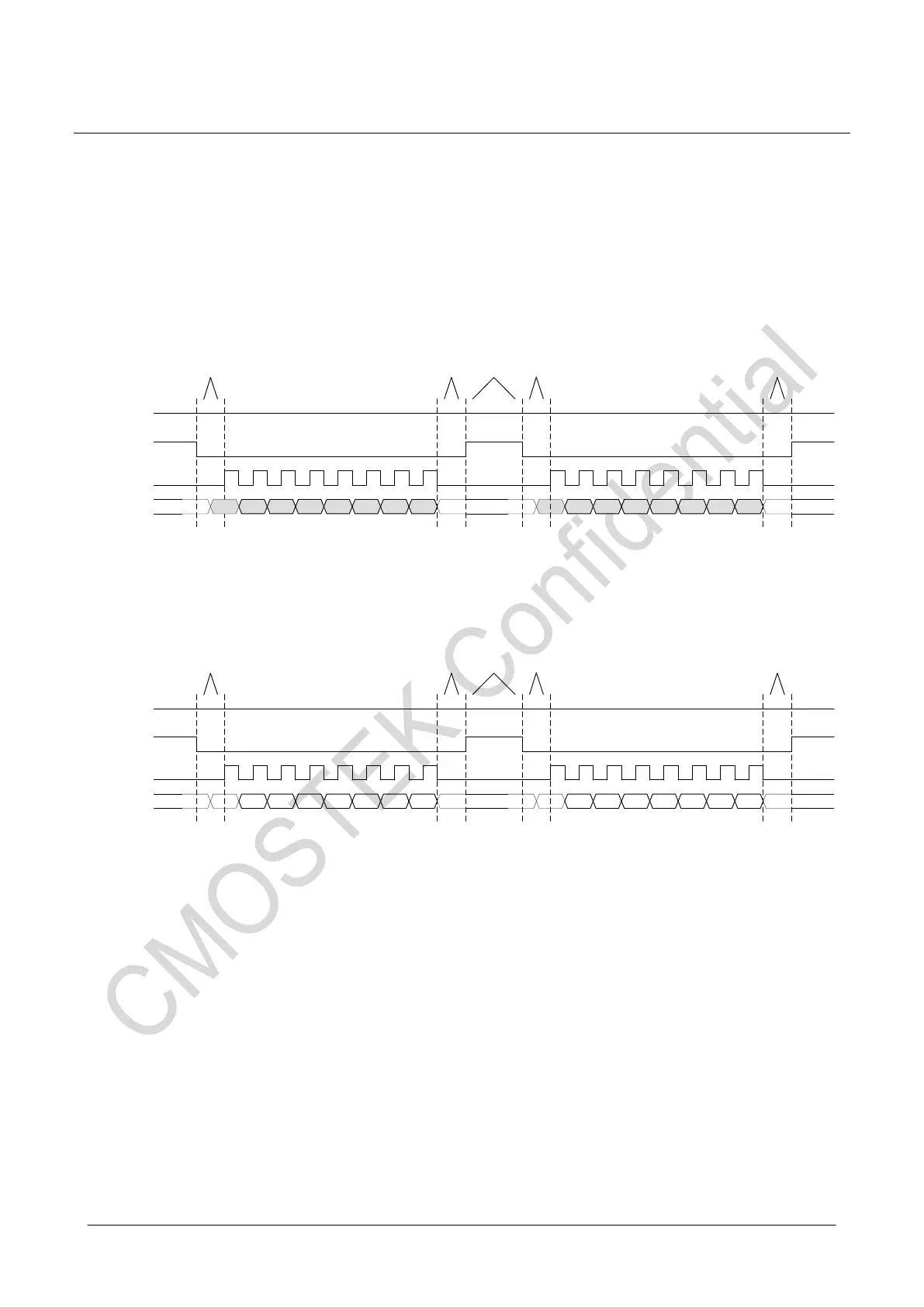
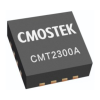
5.2.1 FIFO Read Operation
When the MCU accesses to the FIFO, the user must first configure a few registers to setup the FIFO read/write mode, as well as
some other working mode. The details are introduced in “AN143-CMT2219B FIFO and Data Packet Usage Guideline”. Here is the
read-write timing diagram. Note that there is a slight difference in the control of the FCSB for accessing to the FIFO and the control
of the CSB for accessing to the register. When the MCU starts to access to the FIFO, FCSB must be pulled down 1-clock cycle at
first, and then send the rising edge of SCL. After the last falling edge of SCL is sent, the MCU must wait at least 2 us to pull up the
FCSB. Between the adjacent read/write operations, the FCSB must be pulled high for 4us at least. When writing the FIFO, the first
bit data must be ready 0.5 clock cycles before sending the first rising edge of SCL.
SCLK
FCSB
SDIO
X X
FIFO read data
01234567 01234567X
FIFO read data
CSB
> 1 SCLK cycle > 4 us> 2 us > 2 us> 1 SCLK cycle
Figure 11. SPI read FIFO timing
SCLK
FCSB
SDIO
X X
FIFO write data
01234567 01234567X
FIFO write data
CSB
> 1 SCLK cycle > 4 us> 2 us > 2 us> 1 SCLK cycle
Figure 12. SPI write FIFO timing