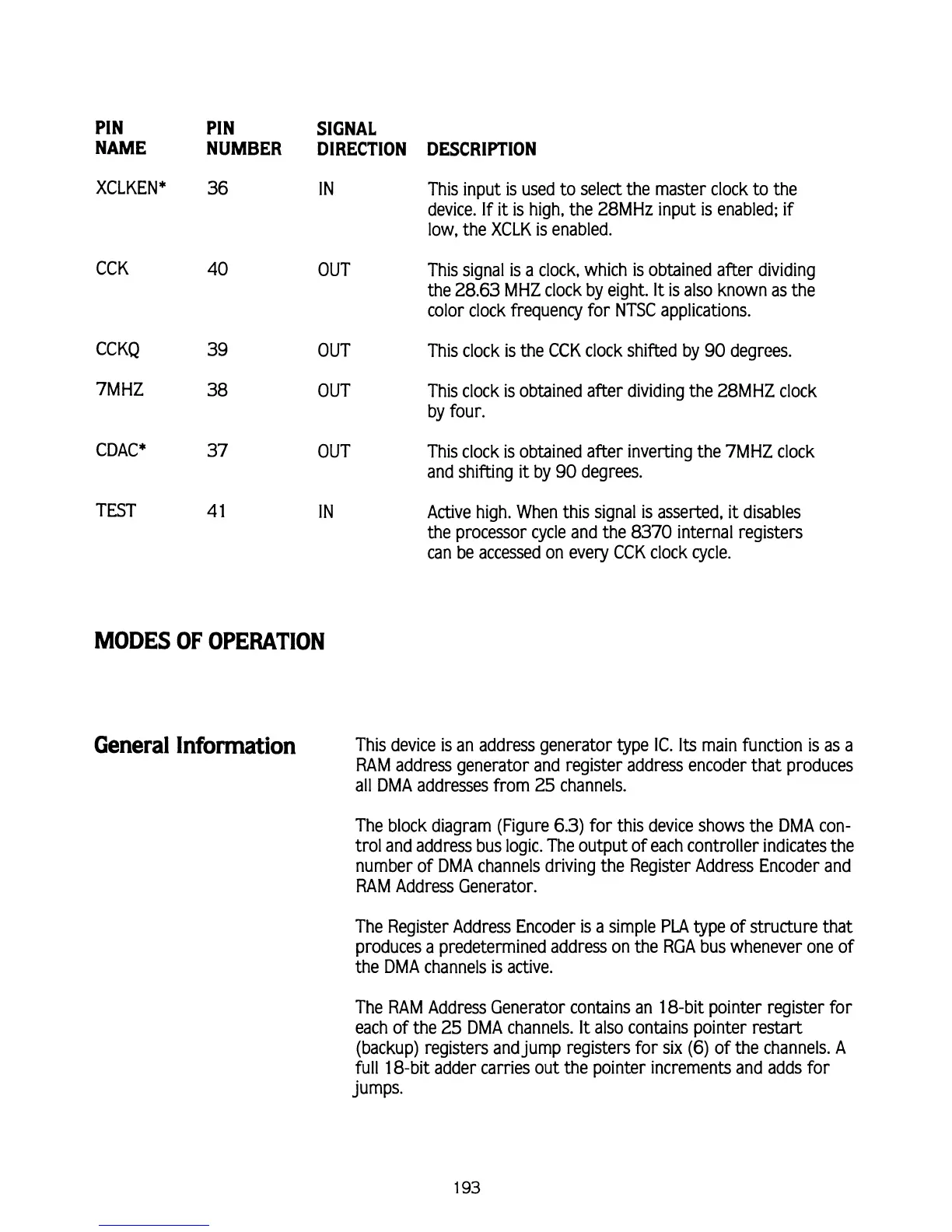
PIN
NAME
XCLKEN*
CCK
CCKQ
7MHZ
CDAC*
TEST
PIN
NUMBER
SIGNAL
DIRECTION DESCRIPTION
IN
This input is used to select the master clock to the
device. If
it
is high, the 28MHz input is enabled; if
low. the XCLK is enabled.
OUT This signal is a clock, which is obtained after dividing
the 28.63 MHZ clock by eight.
It
is also known as the
color clock frequency for NTSC applications.
OUT This clock is the
CCK
clock shifted by
90
degrees.
OUT This clock is obtained after dividing the
28MHZ clock
by four.
OUT This clock is obtained after inverting the 7MHZ clock
and shifting
it
by
90
degrees.
IN
Active high. When this signal is asserted,
it
disables
the processor cycle and the 8370 internal registers
can be accessed on every CCK clock cycle.
MODES OF OPERATION
General
information
This device is an address generator type IC.
Its
main function is as a
RAM
address generator and register address encoder that produces
all
DMA
addresses from 25 channels.
The block diagram (Figure 6.3) for this device shows the
DMA
con-
trol and address bus logic. The output of each controller indicates the
number of
DMA
channels driving the Register Address Encoder and
RAM
Address Generator.
The Register Address Encoder is a simple
PM
type of structure that
produces a predetermined address on the RGA bus whenever one of
the
DMA
channels is active.
The
RAM
Address Generator contains an 18-bit pointer register for
each of the 25
DMA
channels.
It
also contains pointer restart
(backup) registers and jump registers for six
(6)
of the channels.
A
full 18-bit adder carries out the pointer increments and adds for
jumps.