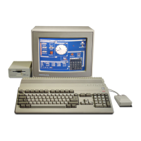
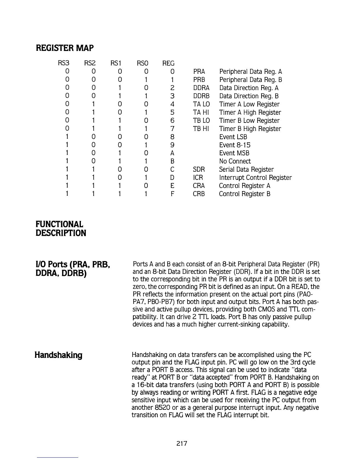
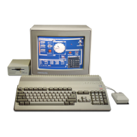
REGISTER MAP
RS3
RS2 RS1
RSO REG
0
0
0
0 0
0 0
0
1
1
0
0
1
0
2
0
0
1
1
3
0
1
0 0
4
0
1
0
1
5
0
1
1
0
6
0
1
1
1
7
1
0 0
0
8
1
0
0
1
9
1
0
1
0
A
1
0
1
1
B
1
1
0
0
C
1
1
0
1
D
1
1
1
0
E
1
1
1
1
F
PRA
PRB
DDRA
DDRB
TA
L0
TA
HI
TB
L0
TB
HI
SDR
ICR
CRA
CRB
Peripheral Data Reg.
A
Peripheral Data Reg.
B
Data Direction Reg.
A
Data Direction Reg.
B
Timer
A
Low Register
Timer
A
High Register
Timer
B
Low Register
Timer
B
High Register
Event LSB
Event
8-
1
5
Event MSB
No Connect
Serial Data Register
Interrupt Control Register
Control Register
A
Control Register B
FUNCTIONAL
DESCRIPTION
U0
Ports
(PM, PRB,
Ports
A
and
B
each consist of an 8-bit Peripheral Data Register (PR)
DDRA, DDRB)
and an 8-bit Data Direction Register (DDR). If a bit in the DDR
is
set
to the corresponding bit in the PR
is
an output if a DDR bit is set to
zero, the corresponding PR bit is defined as an input. On a READ, the
PR reflects the information present on the actual port pins
(PAO-
PA7, PBO-PB7) for both input and output bits. Port
A
has both pas-
sive and active
pullup devices, providing both CMOS and TTL com-
patibility.
It
can drive 2 TTL loads. Port B has only passive pullup
devices and has a much higher current-sinking capability.
Handshaking
Handshaking on data transfers can be accomplished using the PC
output pin and the
FLAG
input pin. PC will go low on the 3rd cycle
after a PORT B access. This signal can be used to indicate "data
ready" at PORT B or "data accepted" from PORT B. Handshaking on
a 16-bit data transfers (using both PORT
A
and PORT B)
is
possible
by always reading
or
writing PORT
A
first.
FLAG
is
a negative edge
sensitive input which can be used for receiving the PC output from
another 8520 or as a general purpose interrupt input. Any negative
transition on
FLAG
will set the
FLAG
interrupt bit.