Name Function
TMP88CU74F Terminal Function
Pin
No.
1 P02/S01 RDS RESET O C Z L RDS reset output (LC7074)
2 P03 OSD RST O C Z H OSD control output (M35015)
3 P04 ST/MONO O C Z L STEREO/MONO control signal, L: STEREO
4 P05 PLFL DATA O C Z L PLL, FL control terminal (LC72131 & LC75721NE)
5 P06 PLL STB O C Z L PLL control terminal (LC72131)
6 P07 PLFL CLK O C Z L PLL, FL control terminal (LC72131 & LC75721NE)
7 Vss Vss I GND L GND
8 Xout Xout O XTAL
9 Xin Xin I XTAL
10 RESET_ RESET_ I Eu Lv L Reset input
11 P22/XTOUT TUNED_ I Eu Lv Z Tuning detect, L: Tuned
12 P21/XTIN STEREO_ I Eu Lv Z L: At stereo receive
13 TEST TEST I GND S Connect to GND
14 P20/INT5_ B.DOWN_ I Eu Lv Z Power down detect, L: Power down
15 P10/INT0_ PROTECT_ I Ed E&L Z PROTECTION detect input, H: Detect
16 P11/INT1 RDS START I Z L RDS data input (LC7074)
17 P12 OSD CLK O C Z H OSD control output (M35015)
18 P13 OSD CS O C Z H OSD control output (M35015)
19 P14 OSD DATA O C Z L OSD control output (M35015)
20 P15/INT3 REMOCON I Ed E&L Z Remote control signal input
21 P16/INT2 ACK O C Z L MAIN-SUB CPU comm. control terminal
22 P17/INT4 REQ I Eu Z L MAIN-SUB CPU comm. control terminal
23 P30/SCL SI I MAIN-SUB CPU comm. control terminal
24 P31/SDA SO O C MAIN-SUB CPU comm. control terminal
25 P32/SCK0_ CLK O C MAIN-SUB CPU comm. control terminal
26 P40/AIN0 MODE I Eu Lv Z Destination switching input
27 P41/AIN1 KEY1 I Eu Lv Z Button input 1
28 P42/AIN2 KEY2 I Eu Lv Z Button input 2
29 P43/AIN3 KEY3 I Eu Lv Z Button input 3
30 P44/AIN4 FUNC STB1 O C ZL
Function control output, REC OUT (TC9274-011), EXT/SOURCE (TC9274-012)
31 P45/AIN5 FUNC/T. CON CLK O C ZL
Function control output (TC9274N, TC9273), TONE control output (TC9184P)
32 P46/AIN6 FUNC/T. CON DATA O C ZL
Function control output (TC9274N, TC9273), TONE control output (TC9184P)
33 P47/AIN7 E.VOL STB2 O C Z L Multi Elect. volume control output (TC9459)
34 P50/AIN8 E.VOL STB1 O C L L Elect. volume control output (TC9459)
35 P51/AIN9 TONE STB O C L L TONE control output (TC9184P)
36 P52/AIN10 E.VOL DATA O C L H Elect. volume control output (TC9459)
37 P53/AIN11 E.VOL CLK O C L H Elect. volume control output (TC9459)
Symbol I/O Type Op Det Res Init
SEMICONDUCTORS
!!
!!
! IC’s
Note: Abbreviation ahead of IC No. indicates the name of P.W.B.
PO: Power P.W.B. RE: Regulator P.W.B.
EX: Exit in P.W.B. AU: Audio/DSP P.W.B.
CO: Control P.W.B. AC: Amp Connect P.W.B
TMP88CU74F
(CO: IC303)
Function
38 VASS VASS I Ref. volt (GND)
39 VAREF VAREF I Ref. volt (VDD)
40 VDD VDD I Power supply
41 P60 FL CE O P Ed S L H FL display control output (LC75721NE)
42 P61 FL RES O P Ed S L H FL display control output (LC75721NE)
43 P62 FUNC STB2 O P Ed Z L Function control output (TC9273), INPUT (TC9273)
44 P63 SA-RELAY O P Id L L Surround SP relay A control terminal, L: Mute
45 P64 SB-RELAY O P Id L L Surround SP relay B control terminal, L: Mute
46 P65 C-RELAY O P Id L L Center SP relay control terminal, L: Mute
47 P66 F-RELAY O P Id L H Front SP relay control terminal, L: Mute
48 P67 PRE F MUTE O P Ed L H Front PRE OUT mute control terminal, L: Mute
49 P70 PRE C MUTE O P Ed L L Center PRE OUT mute control terminal, L: Mute
50 P71 PRE S MUTE O P Ed L L Surround PRE OUT mute control terminal, L: Mute
51 P72
SUB WOOFER MUTE
OPEd L H Sub-woofer PRE OUT mute control terminal, L: Mute
52 P73 H/P RELAY O P Id L H H/P OUT relay control terminal, L: Mute
53 P74 EXP OE O P Ed L H Port expander control terminal (BU4094)
54 P75 EXP CLK O P Ed L L Port expander control terminal (BU4094)
55 P76 EXP DATA O P Ed L L Port expander control terminal (BU4094)
56 P77 EXP STB O P Ed L L Port expander control terminal (BU4094)
57 P80 POWER O P Id L H Power relay control output, H: ON
58 P81 RESET2 O P Id L L Reset signal output to sub-CPU, H: Reset
59 P82 PRE S.BACK MUTE O P Id L L Surround Back PRE PUT mute control terminal, L: Mute
60 P83 S.BACK VOL MUTE O P Id L L Surround Back volume mute, L: Mute
61 P84 STANDBY O P Id L H Standby LED drive output H: Light
62 P85 S.BACK RELAY O P Id L L Surround Back SP relay control terminal, L: Mute
63 P86 LED CK O P Id L L LED control terminal (BU2090F)
64 P87 LED DATA O P Id L L LED control terminal (BU2090F)
65 P90 TUNER MUTE O P Ed L H TUNER mute control terminal, H: Mute
66 P91 MULTI MUTE O P Id L H MULTI PREOUT mute control terminal, H: Mute
67 P92 S MONI DET I Eu Lv Z S monitor connection detect input, L: Connected
68 P93 S SIG DET I Eu Lv Z S signal detect input, H: Detected
69 P94 SYNC DET. I Eu Lv Z Sync detect input, H: Ext. sync
70 P95 SEL A (M) I Eu Lv Z Master volume rotation detect input (rotary encoder)
71 P96 SEL B (M) I Eu Lv Z Master volume rotation detect input (rotary encoder)
72 P97 CINEMA EQ O P Eu Lv Z L CINEMA EQ control output, H: ON
73 PD0 VOL MUTE O P Ed L L Master volume minimum control, L: Min.
74 PD1 SEL C (S) I Eu Lv Z Surround mode rotation detect input (rotary encoder)
75 PD2 SEL D (S) I Eu Lv Z Surround mode rotation detect input (rotary encoder)
76 PD3 SEL E (F) I Eu Lv Z
Input selector switch rotation detect input (rotary encoder)
77 PD4 SEL F (F) I Eu Lv Z
Input selector switch rotation detect input (rotary encoder)
78 Vkk Vkk GND fixed
79 P00/SCK1_ RDS CLK I SZ RDS clock input (LC7074)
80 P01/SI1 RDS DATA I SZ RDS data input (LC7074)
I/O Type Op Det Res Init
Name
Pin
No.
Symbol
NOTE:
Pin No. : Terminal number of microcomputer.
Port Name : The name entered in the data sheet of microcomputer.
Symbol : Symbolized interface function.
I/O : Input or out of part.
“I” = Input port
“O” = Output port
Type : Composition of port in case of output port.
“C” = CMOS output
“N” = NMOS open drain output
“P” = PMOS open drain output
Op : Pull up/Pull down selection information.
“Iu” = Inner microcomputer pull up
“Id” = Inner microcomputer pull down
“Eu”= External microcomputer pull up
“Ed”= External microcomputer pull down
Det : Indicates judging state of input port. Level detection is “LV”; Edge detection is “Ed”; Detection by both shifting is “E&L”;
Serial data detection is “S” (Serial data output is also “S”).
Res : State at reset.
“H” = Outputs High Level at reset
“L” = Outputs Low Level at reset
“Z” = Becomes High impedance mode at reset
Ini : Initial output state.
Function : Function and logical level explanation of signals to be interface.
124
25
40
41
64
65
80
13
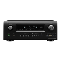
AVR-3801
1TMP88CU74F.p65 00/09/12, 15:15Page 12-13 AdobePageMaker6.5J/Win
 Loading...