


K
Kathryn LeeSep 8, 2025
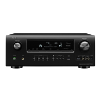
What does 'antenna error' mean on my Denon Stereo Receiver?
- MMs. Nancy DeanSep 8, 2025
The message “ANTENNA ERROR” indicates that the antenna is not connected. Check that the connections are correct.
What does 'antenna error' mean on my Denon Stereo Receiver?
The message “ANTENNA ERROR” indicates that the antenna is not connected. Check that the connections are correct.
How to fix no audio output with HDMI connection on Denon Stereo Receiver?
First, check the connection of the HDMI connectors. If you want to output HDMI audio from the speakers, set “HDMI Audio Out” on the menu to “AMP.” If you want to output HDMI audio from a TV, set “HDMI Audio Out” on the menu to “TV.”
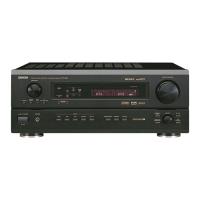
Why is there no sound produced from my surround speaker on Denon AVR-3311CI?
Check if the surround speakers are connected to the SURROUND terminals.
Why is there no sound from the front height speaker on my Denon AVR-3311CI Stereo Receiver?
To resolve this, set “Surround Parameter” – “F.Height” on the menu to “ON.” Also, ensure “Amp Assign” is set to “Normal” and “Speaker Config.” – “Surround” is set to something other than “None.”
Why is there no sound from the surround back speaker on my Denon AVR-3311CI?
First, set “Amp Assign” on the menu to “Normal.” Next, ensure “Speaker Config.” – “S.Back” on the menu is set to something other than “None.” Also, verify that “Surround Parameter” – “S.Back” on the menu is set to something other than “OFF.” Lastly, make sure the surround mode is not set to “STEREO.”
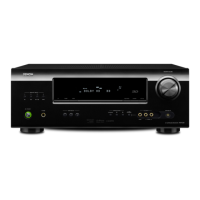
Why no picture appears on my Denon Stereo Receiver?
Check the TV connection and set the TV input correctly.
After turning on the power, why is the power indicator blinking red on my Denon AVR-3311CI Stereo Receiver?
Turn off the power and please contact the DENON service adviser, because this indicates that the unit amplifier circuit has failed.
Why can't I login to Napster on my Denon AVR-3311CI Stereo Receiver?
Login information may be incorrect. Check if the Username for Napster has been properly entered and re-enter the Password. (Note: Password is not displayed.)
What does 'no signal' mean on my Denon AVR-3311CI?
The message “NO SIGNAL” indicates that the antenna is not connected. Check that the connections are correct.
What to do if my Denon AVR-3311CI does not turn on?
First, check whether the power plug is correctly inserted into the power outlet. If it is, the protection circuit may be active. Disconnect the power plug from the electric outlet, wait 5 to 10 seconds, and then reinsert it.
Checks leakage current and resistance for safety compliance.
Details power amplifier, analog, digital, and phono specifications.
Details standard and component video connector specs.
Specifications for HD Radio reception.
Specifications for FM/AM tuner reception.
Power supply, power consumption, dimensions, and weight.
Procedure for initializing the μcom before replacing digital PWB.
Steps for initializing the receiver's μcom and peripherals.
Instructions for connecting the PCB HDMI JIG for servicing.
Steps for disassembling the front panel assembly.
Steps for disassembling the heat sink assembly.
Steps for disassembling the PCB REG CNT/PCB REG.
Steps for disassembling the HDMI unit assembly.
Steps for disassembling the main transformer unit.
Details how to press ON/STANDBY with other buttons to access special modes.
Describes how to enter and use the µcom/DSP version display mode.
Explains the sequence of information displayed in the version mode.
How to start and use the error mode to display protection history.
Explains the history display format and meaning of different codes.
Explains POWER LED flashing patterns for protection incidents.
How to start the diagnostic mode using buttons.
How to cancel the diagnostic mode.
How to perform remote operations in diagnostic mode.
Lists items to confirm for video signal paths.
Confirmation steps for analog signal paths in different zones.
Confirmation steps for digital signal paths in the main zone.
Confirmation steps for digital signal paths in ZONE2.
Confirmation steps for digital signal paths in ZONE3.
Confirmation steps for HDMI signal paths.
Procedure for adjusting idling current for audio section.
Troubleshooting steps for power-related issues.
Troubleshooting flow for CVBS monitor output issues.
Troubleshooting flow for Component monitor output issues.
Troubleshooting steps for HDMI/DVI connection issues resulting in no picture/sound.
Troubleshooting procedure for audio output issues.
Troubleshooting steps for network connectivity issues.
Illustrates signal levels for the front channel.
Illustrates signal levels for the center channel.
Illustrates signal levels for the subwoofer channel.
Illustrates signal levels for the surround channel.
Illustrates signal levels for the surround back channel.
Illustrates signal levels for ZONE2/3.
Component layout of the 7CH AMP PCB.
Foil layout of the 7CH AMP PCB.
Foil layout of the SMPS PCB.
Foil layout of the speaker PCB.
Foil layout of the REG PCB.
Foil layout of the FRONT_CNT PCB.
Foil layout of the REG_CNT PCB.
Foil layout of the SIDE_CNT PCB.
Foil layout of the USB PCB.
Foil layout of the MIC PCB.
Foil layout of the FRONT PCB.
Foil layout of the FUNCTION_CNT PCB.
Foil layout of the VAUX PCB.
Foil layout of the VIDEO PCB.
Foil layout of the FUNCTION PCB.
Foil layout of the HDMI PCB.
Foil layout of the FRONT HDMI PCB.
Foil layout of the AUDIO[INPUT] PCB.
Foil layout of the PREOUT PCB.
Foil layout of the SMPS PCB.
Wiring diagram and pin assignments for REG_SIRIUS_COMMON.
Wiring diagram and pin assignments for REG_SIRIUS_COMMON.
Wiring for SIRIUS, RS232C, and trigger connections.
Wiring diagram and pin assignments for REG_SIRIUS_COMMON.
Foil layout of the HDMI PCB.
Foil layout of the FRONT HDMI PCB.
List of semiconductor parts used in the exploded view.
List of capacitor parts used in the exploded view.
List of miscellaneous other parts.
List of screws used in the unit.
List of wires and cables used in the unit.
Details of major semiconductors (ICs) used in the unit.
| Channels | 7.2 |
|---|---|
| Amplifier Type | Discrete |
| Power Output (8 ohms) | 125 W |
| HDMI Inputs | 6 |
| HDMI Outputs | 2 |
| Response Bandwidth | 10 Hz - 100 kHz |
| Signal-To-Noise Ratio | 102 dB |
| THD | 0.05 % |
| Input Impedance | 47 kOhms |
| Input Sensitivity | 200 mV |
| Tuner Type | Digital |
| Tuner Bands | AM/FM |
| HDMI Switching | Yes |
| 3D Technology | Yes |
| Audio D/A Converter | 192kHz/24-bit |
| Digital Sound Processor (DSP) | Yes |
| DSP Preset Qty | 7 |
| Frequency Response | 10 Hz - 100 kHz |
| HDMI Version | 1.4a |
| USB Port | Yes |
| Audio Formats Supported | Dolby TrueHD, DTS-HD Master Audio |
| Network Connectivity | Ethernet |
| Video Inputs | 3 |
| Video Outputs | 1 |
| Audio Outputs | 2 |
| HDMI Features | ARC, CEC |
| Supported Video Formats | 1080p |