PIN
DESCRIPTION
NO. NAME I/O
5-V
TOLERANT
26 MS/ADR1 I Yes Software control I/F, SPI chip select / I2C slave address
setting1(2)
27 MODE I No Control mode setting, (see the Serial Control Mode section,
Control Mode Pin Setting)
28 RXIN7/ADIN0 I Yes Biphase signal, input 7 / AUXIN0, serial audio data input(2)
29 RXIN6/ALRCKI0 I Yes Biphase signal, input 6 / AUXIN0, LR clock input(2)
30 RXIN5/ABCKI0 I Yes Biphase signal, input 5 / AUXIN0, bit clock input(2)
31 RXIN4/ASCKI0 I Yes Biphase signal, input 4 / AUXIN0, system clock input(2)
32 RXIN3 I Yes Biphase signal, input 3(2)
33 RXIN2 I Yes Biphase signal, input 2(2)
34 RST I Yes Reset Input, active low(2) (4)
35 RXIN1 I Yes Biphase signal, input 1, built-in coaxial amplier
36 VDDRX – – Power supply, 3.3 V (typ.), for RXIN0 and RXIN1.
37 RXIN0 I Yes Biphase signal, input 0, built-in coaxial amplier
38 GNDRX - - Ground, for RXIN
39 XTI I No Oscillation circuit input for crystal resonator or external XTI
clock source input(5)
40 XTO O No Oscillation circuit output for crystal resonator
41 AGND – – Ground, for PLL analog
42 VCC – – Power supply, 3.3 V (typ.), for PLL analog
43 FILT O No External PLL loop filter connection terminal; must connect
recommended lter
44 VCOM O No ADC common voltage output; must connect external
decoupling capacitor
45 AGNDAD – – Ground, for ADC analog
46 VCCAD – – Power supply, 5.0 V (typ.), for ADC analog
47 VINL I No ADC analog voltage input, left channel
48 VINR I No ADC analog voltage input, right channel
(1) Schmitt trigger input
(2) Schmitt trigger input
(3) Open-drain conguration in I2C mode
(4) Onboard pull-down resistor (50 k Ω , typical)
(5) CMOS Schmitt trigger input
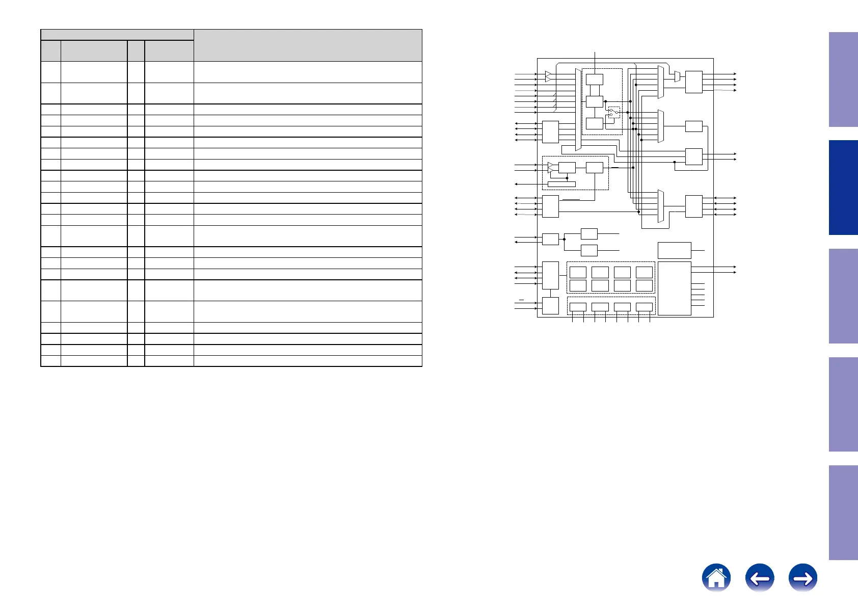
BLOCK DIAGRAM
Clock/ Data
Recovery
MPIO_A
SELECTOR
MPIO_C
SELECTOR
MPIO _B
SELECTOR
ADC
Com. Supply
MPO0/1
SELECTOR
MPO 0
MPO 1
MAIN
OUTPUT
SCKO
BCK
LRCK
DOUT
PORT
RXIN8
RXIN9
RXIN10
RXIN11
DITOUT
AUTO
DIR
ADC
AUXIN0
AUXIN1
AUXIN2
AUTO
DIR
ADC
AUXIN0
AUXIN1
AUXIN2
AUTO
DIR
ADC
AUXIN0
AUXIN1
DIT
Lock:DIR
Unlock:ADC
AUXIN 2
AUXOUT
OSC
Divider
XMCKO
Divider
XMCKO
DITOUT
RECOUT0
RECOUT1
AUXIN 0
AUXIN1
ADC Standalone
ADC Mode
Control
Function
Control
REGISTER
POWER SUPPLY
MC /SCL
MDI /SDA
MDO /ADR0
MS/ADR 1
FILT
PLL
DIR
Lock Detection
ERROR /INT0
NPCM /INT1
ADC Clock
(SCK/BCK /LRCK)
(To MPIO_A & MPO0/ 1 )
ADC
MODE
DIR CS
(48-bit )
DIT CS
(48-bit )
DIR Interrupt
GPIO/GPO
Data
MPIO_A
MPIO_B
MPIO_C
MPO0
MPO1
Divider
(to MPIO_A )
Secondary BCK/ LRCK
Selector
RECOUT0
RECOUT1
SBCK /SLRCK
DOUT
RXIN7
SCKO/BCK/LRCK
RXIN 0
RXIN 1
RXIN 2
RXIN 4/ASCKI0
RXIN 3
RXIN 5/ABCKI0
RXIN 6/ALRCKI 0
RXIN 7/ADIN0 RXIN7
RXIN6
RXIN5
RXIN4
RXIN3
RXIN2
RXIN1
RXIN0
MPIO_A0
MPIO_A1
MPIO_A2
MPIO_A3
VINL
VINR
VCOM
MPIO _C0
MPIO _C1
MPIO _C2
MPIO _C3
XTI
XTO
AGND VDDRX GNDRX DVDDVCCAD AGNDAD DGNDVCC
ADC
ANALOG
DIR
ANALOG
ALL
DIR
ANALOG
SPI/I C
INTERFACE
2
Reset
and Mode
Set
All Port
f Calculator
S
DIR
f Calculator
S
DIR
P and P
CD
EXTRA DIR FUNCTIONS
f Calculator
S
ERROR DETECTION
Non-PCM DETECTION
Flags
DTS-CD/LD Detection
Validity Flag
User Data
Channel Status Data
BFRAME Detection
Interrupt System
MPIO_B3
MPIO_B2
MPIO_B1
MPIO_B0
RST
PCM9211
www.ti.com
SBAS495 –JUNE 2010
BLOCK DIAGRAM
Copyright © 2010, Texas Instruments Incorporated Submit Documentation Feedback 9
Product Folder Link(s): PCM9211
58
Caution in
servicing
Electrical Mechanical Repair Information Updating
 Loading...