No. Pin Name I/O Function PD State
15
CAD0_I2C I Chip Address 0 Pin in I2C Bus serial control mode
Hi-Z
CSN I Chip Select Pin in 3-wire serial control mode
DIF I Audio Data Format Select in Parallel control mode. "L": 32-bit MSB, "H": 32-bit I2S
16
PS I
(I2C pin = "H") Control Mode Select Pin "L": I2C Bus serial control mode, "H": Parallel control
mode.
Hi-Z
CAD0_SPI I (I2C pin = "L") Chip Address 0 Pin in 3-wire serial control mode
17 I2C I
Control Mode Select Pin "L": 3-wire serial control mode
"H": I2C Bus serial control mode or Parallel control mode.
Hi-Z
18 AOUTL1P O Lch Positive Analog Output 1 Pin Hi-Z
19 AOUTL1N O Lch Negative Analog Output 1 Pin Hi-Z
20 VREFL1 I Negative Voltage Reference Input Pin, AVSS Hi-Z
21 VREFH1 I Positive Voltage Reference Input Pin, AVDD Hi-Z
22 AOUTR1N O Rch Negative Analog Output 1 Pin Hi-Z
23 AOUTR1P O Rch Positive Analog Output 1 Pin Hi-Z
24 AOUTL2P O Lch Positive Analog Output 2 Pin Hi-Z
25 AOUTL2N O Lch Negative Analog Output 2 Pin Hi-Z
26 VREFL2 I Negative Voltage Reference Input Pin, AVSS Hi-Z
27 VREFH2 I Positive Voltage Reference Input Pin, AVDD Hi-Z
28 AOUTR2N O Rch Negative Analog Output 2 Pin Hi-Z
29 AOUTR2P O Rch Positive Analog Output 2 Pin Hi-Z
30 AVSS - Analog Ground Pin -
31 AVDD - Analog Power Supply Pin, 3.0V-5.5V -
32 AOUTL3P O Lch Positive Analog Output 3 Pin Hi-Z
33 AOUTL3N O Lch Negative Analog Output 3 Pin Hi-Z
34 VREFH3 I Positive Voltage Reference Input Pin, AVDD Hi-Z
35 VREFL3 I Negative Voltage Reference Input Pin, AVSS Hi-Z
36 AOUTR3N O Rch Negative Analog Output 3 Pin Hi-Z
37 AOUTR3P O Rch Positive Analog Output 3Pin Hi-Z
38 AOUTL4P O Lch Positive Analog Output 4 Pin Hi-Z
39 AOUTL4N O Lch Negative Analog Output 4 Pin Hi-Z
40 VREFH4 I Positive Voltage Reference Input Pin, AVDD Hi-Z
41 VREFL4 I Negative Voltage Reference Input Pin, AVSS Hi-Z
42 AOUTR4N O Rch Negative Analog Output 4 Pin Hi-Z
43 AOUTR4P O Rch Positive Analog Output 4 Pin Hi-Z
44 LDOE I Internal LDO Enable Pin. "L": Disable, "H": Enable Hi-Z
45 TVDD - Digital Power Supply Pin, 3.0V-3.6V -
46 DVSS - Digital Ground Pin -
47 VDD18
O LDO Output Pin (LDOE pin = "H") This pin should be connected to DVSS with 1.0µF.
(Note 4)
I 1.8V Power Input Pin (LDOE pin = "L")
48 PDN I
Power-Down & Reset Pin
When this pin is "L", the AK4458 is powered-down and the control registers are reset to default
state.
Hi-Z
Note 2. All input pins except internal pull-up/down pins should not be left oating.
Note 3. PCM mode and DSD mode are controlled by registers. Daisy Chain mode is controlled by both
registers and pins.
Note 4. This pin outputs DVSS when the LDOE pin = "H" and Hi-z when the LDOE pin = "L".
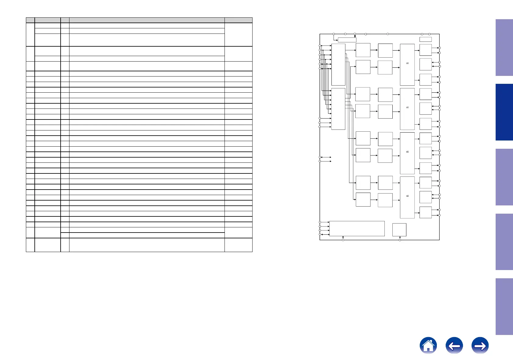
FUNCTIONAL BLOCK DIAGRAM
[AK4458]
014011794-E-00 2015/01
- 5 -
4. Block Diagram and Functions
MCLK
SDTI1/DSDR1
LRCK/DSDL1
CAD0_I2C/CSN/DIF
BICK/DCLK
SCL/CCLK/TDM1
SDA/CDTI/TDM0
PDN AVDD
Clock
Divider
DVSS TVDD
PS/CAD0_SPI
AOUTR1N
VREFH1
VREFL1
AVSS
AOUTL1P
AOUTR1P
PCM
Data
Interface
De-empha
sis
DSD
Data
Interface
8X
Interpolator
Control
Register
SCF
SCF
AOUTR2N
VREFH2
VREFL2
AOUTL2P
AOUTL2N
AOUTR2P
Vref
SDTI2/DSDL2
8X
Interpolator
SCF
SCF
Vref
Bias
I2C
AOUTR3N
VREFH3
VREFL3
AOUTL3P
AOUTL3N
AOUTR3P
8X
Interpolator
SCF
SCF
AOUTR4N
VREFH4
VREFL4
AOUTL4P
AOUTL4N
AOUTR4P
Vref
8X
Interpolator
SCF
SCF
Vref
SDTI3/DSDR2/TDMO1
SDTI4/DSDL3/TDMO2
DSDR3
DSDL4
DSDR4
VDD18
LDO
DZF/SMUTE
CAD1/DCHAIN
LDOE
DAT T
Soft Mute
DSD Filter
DAT T
Soft Mute
DAT T
Soft Mute
DSD Filter
DAT T
Soft Mute
DATT
Soft Mute
DSD Filter
DAT T
Soft Mute
DAT T
Soft Mute
DSD Filter
DAT T
Soft Mute
Modulator
Noise
Rejection
Filter
Modulator
Noise
Rejection
Filter
Modulator
Noise
Rejection
Filter
Modulator
Noise
Rejection
Filter
AOUTL1N
61
Caution in
servicing
Electrical Mechanical Repair Information Updating
 Loading...