46
S-102
ES6178FF PIN DESCRIPTION
Name Pin Numbers I/O Definition
VEE 1,18, 27, 59, 68, 75,
92, 99, 104, 130,
148, 157, 159, 164,
183, 193, 201
P I/O power supply.
LA[21:0]
2-7, 10-16, 19-23,
204-207
O RISC port address bus.
VSS 8, 17, 26, 34, 43,
60, 67, 76, 84, 91,
98, 103, 120, 129,
138, 147, 156, 163,
171, 177, 184, 192,
200, 208
G Ground.
VCC
9, 35, 44, 83, 121,
139, 172
P Core power supply.
RESET# 24 I Reset input; (5V tolerant input).
TDMDX
25
O TDM transmit data output.
RSEL I LCS3 ROM Boot Data Width Select. Strapped to VCC or ground via 4.7-k:
resistor; read only during reset.
TDMDR 28 I TDM receive data input; (5V tolerant input).
TDMCLK 29 I TDM clock input; (5V tolerant input).
TDMFS 30 I TDM frame sync input; (5V tolerant input).
TDMTSC# 31 O TDM output enable.
TWS
32
O Audio transmit frame sync output.
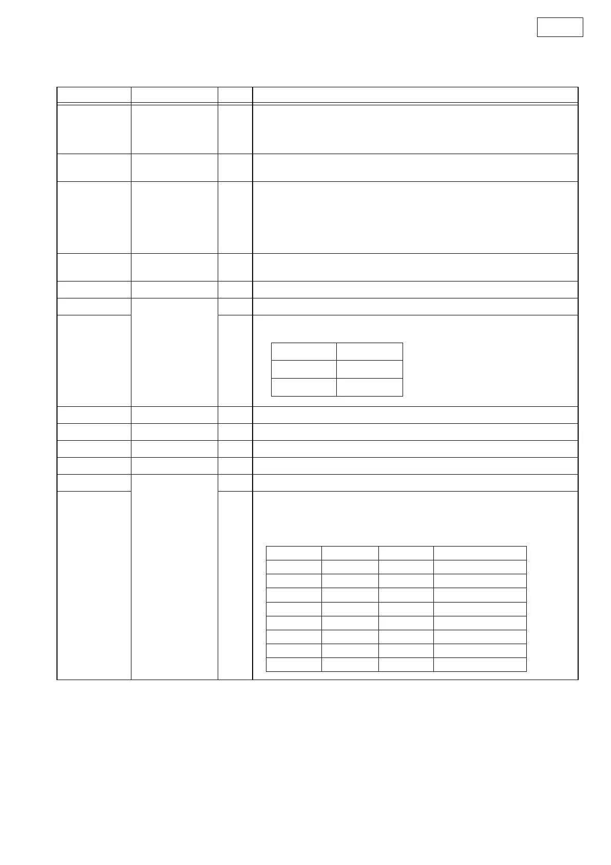
SEL_PLL2 I System and DSCK output clock frequency selection is made at the rising edge of
RESET#. The matrix below lists the available clock frequencies and their
respective PLL bit settings. Strapped to VCC or ground via 4.7-k: resistor; read
only during reset.
RSEL Selection
016-bit ROM
18-bit ROM
SEL_PLL2 SEL_PLL1 SEL_PLL0 PLL Settings
0 0 0 DCLK u.5
0 0 1 DCLK u 5.0
010 Bypass
0 1 1 DCLK u4.0
1 0 0 DCLK u4.25
1 0 1 DCLK u4.75
1 1 0 DCLK u 5.5
1 1 1 DCLK u6.0
 Loading...