■■■■■■■■■■■■■■■■■■■■■■■■■■■■■■■■■■■■■■■■■■■■■■■■■■■■■■■■■■■■■■■■■■■■■■■■■■■■
▼
Signal Connection to External Devices
DS1104 Hardware Installation and Configuration March 2004
143
▲
■■■■■■■■■■I
▲■■■■■■■■■■■■■■■
I/O Circuit and Electrical Characteristics
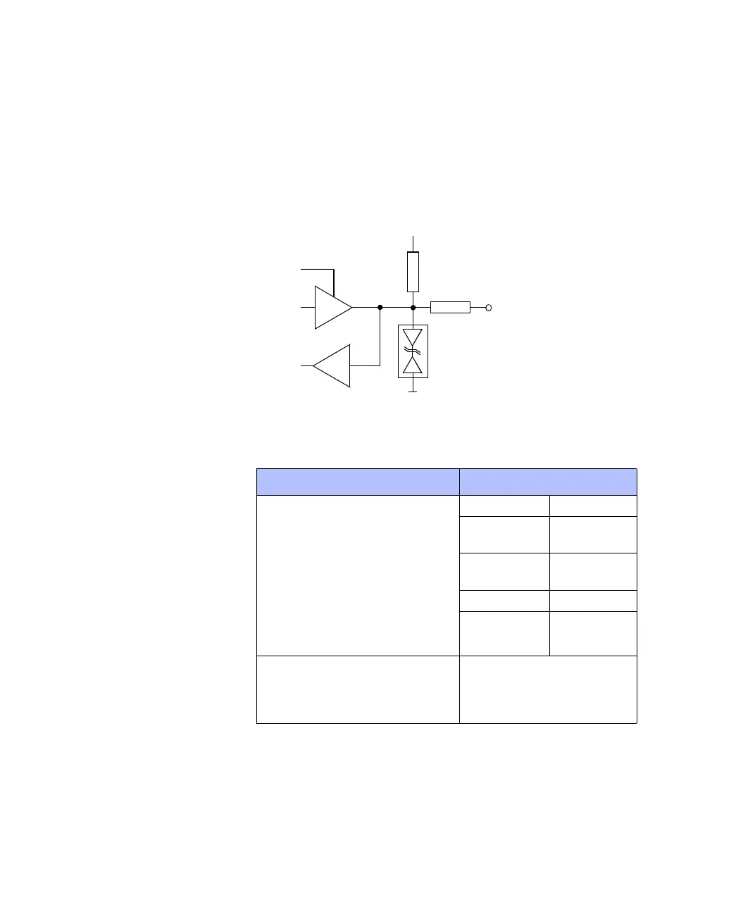
I/O circuit The following illustration is a simplified diagram of the input/output
circuitry of the slave DSP digital I/O.
Electrical characteristics The slave DSP digital I/O have TTL output/input levels with the
following characteristics.
Output
Enable
33
Ω
10 kΩ
VCC
→
I
Slave I/O
Parameter Value
Min. Max.
Input voltage High
Low
2.0 V
0V
5.0 V
0.8 V
Output voltage High
Low
2.4 V
0V
5.0 V
0.4 V
Output current –13 mA +13 mA
Input current
(The current direction is shown in the circuit
diagram above.)
500 µA
Power-up default All digital I/O output circuits
are disabled and driven to
VCC by the built-in 10 kΩ
pull-up resistors.