Contents
Contents
1 Overview 4
2 Schematic Checklist 5
2.1 Power Supply 6
2.1.1 Digital Power Supply 6
2.1.2 Analog Power Supply 6
2.2 Power-on Sequence and System Reset 7
2.2.1 Power-on Sequence 7
2.2.2 Reset 8
2.3 Flash 8
2.4 Clock Source 9
2.4.1 External Clock Source (compulsory) 9
2.4.2 RTC Clock (optional) 10
2.5 RF 11
2.6 UART 11
2.7 ADC 11
2.8 Strapping Pins 11
2.9 GPIO 13
3 PCB Layout Design 16
3.1 General Principles of PCB Layout 16
3.2 Placement of Module on the Base Board 16
3.3 Power Supply 19
3.4 Crystal 20
3.5 RF 21
3.6 Flash 23
3.7 UART 23
3.8 Typical Layout Problems and Solutions 24
3.8.1 Ripple in the power supply is not large, but the RF transmit (TX) performance is rather poor. 24
3.8.2 Ripple in power supply is small during packet transmission, but RF TX performance is still poor. 24
3.8.3 When ESP32-C3 family transmits data packets, the measured power is much higher or lower
than the target power, and the EVM is relatively poor. 24
3.8.4 TX performance is not bad, but the RX sensitivity is low. 24
4 Hardware Development 26
4.1 ESP32-C3-WROOM-1 Module 26
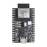
4.2 ESP32-C3 family Development Boards 26
Revision History 27
Solutions, Documentation and Legal Information 28
Espressif Systems 2
Submit Documentation Feedback
ESP32-C3 Family Hardware Design Guidelines V0.5
 Loading...