IN
OUT
Internal
IN
IN
Internal
OUT
ON
OFF
ON
OFF
ON
OFF
ON
ON
OFF
OFF
≧0sec
≧0sec
1sec(typ.)
(*2)
2sec(typ.)
(*1)
T1
1sec(typ.)
(*2)
NOERROR
ON
(=NOALARM)
3. Preparation
SD3 Series Instruction Manual
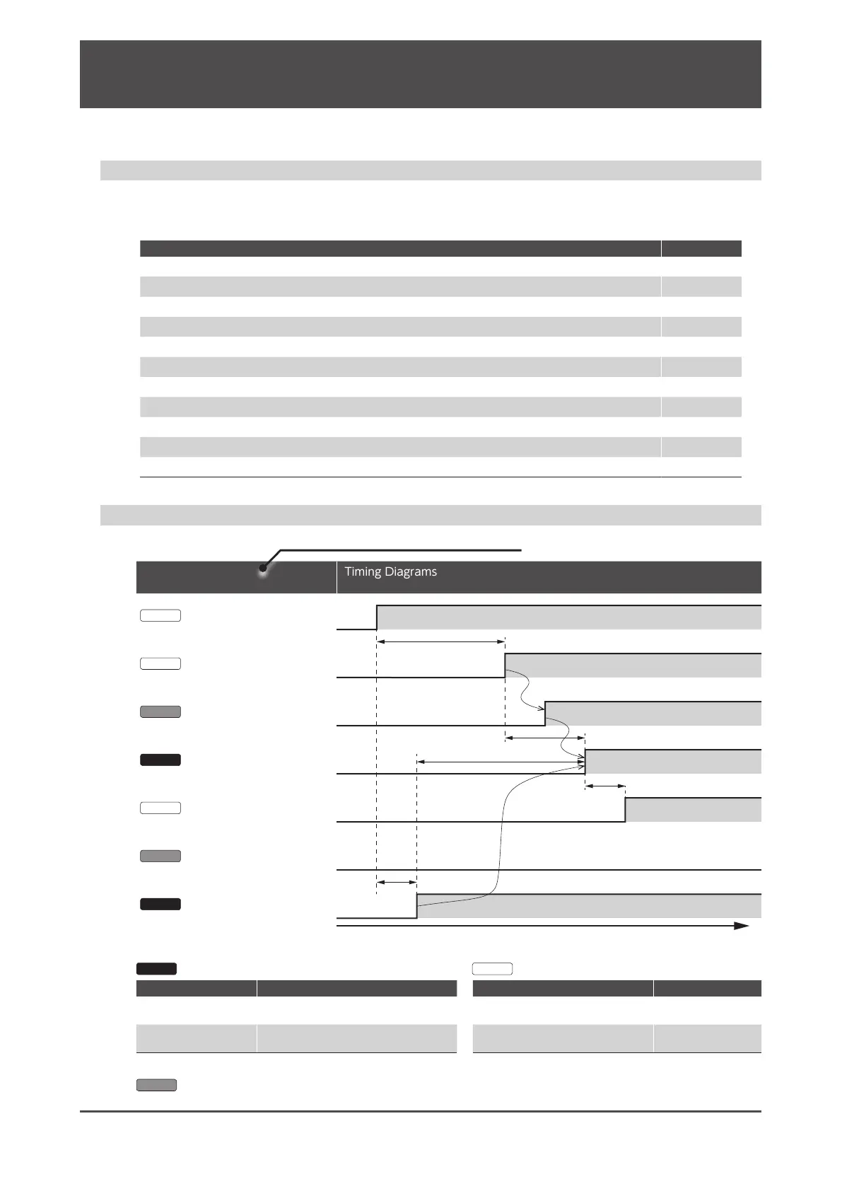
3. Timing Diagrams
List of Timing Diagrams
Description Refer to
Timing Diagram Overview
3. Timing Diagrams
Name
Timing Diagrams
(Output Transistor Status, I/O Input Status, and Internal Status)
DC24V
L1L2L1L2L3
PRDY
SRDY
SVON
-
ALM
Output Transistor I/O Output Status
OFF
ON
Contacts of Input Circuit I/O Input Status
OFF
ON
OUT
IN
Internal
 Loading...