The optimum bias values vary by the device and the needs of the circuit. In general, to
function as an amplifier, the FET needs to have a least a few volts between the Drain and
the Source. If the FET is an N channel type, the Drain must be at least a few volts positive
with respect to Source. If it’s a P channel type, the drain must be negative with respect to
Source.
In addition, the Gate of the FET must be placed at a DC value relative to the Source so that
the current and voltage of the FET is positioned in the linear region between the extremes of
voltage and current – somewhere between all the way on and all the way off. It is in the
middle ground where the distortion is low. Generally for N channel JFETs, it is with the
Gate voltage at 0 or slightly negative with respect to the Source, and for N channel
MOSFETs the gate voltage is a couple volts positive. One of the important functions of a
circuit is to set up the DC conditions of gain stages so that the devices have stable
operation in this region. For every amplifying circuit, there will be a “sweet spot” of voltage
and current which will give the best overall performance.
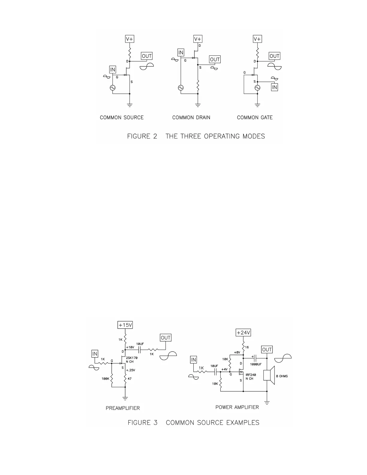
Figure three shows some examples of real circuits that illustrate simple Common-Source
amplifiers and the bias voltages and currents that would be typical for them. You can build
both of these circuits and they will work.
On the left you see an example of a simple preamplifier stage with a gain of roughly 10
times (20 dB). The JFET is self biased in this circuit: With 5 mA going through the JFET,