— 22 —
VX900T
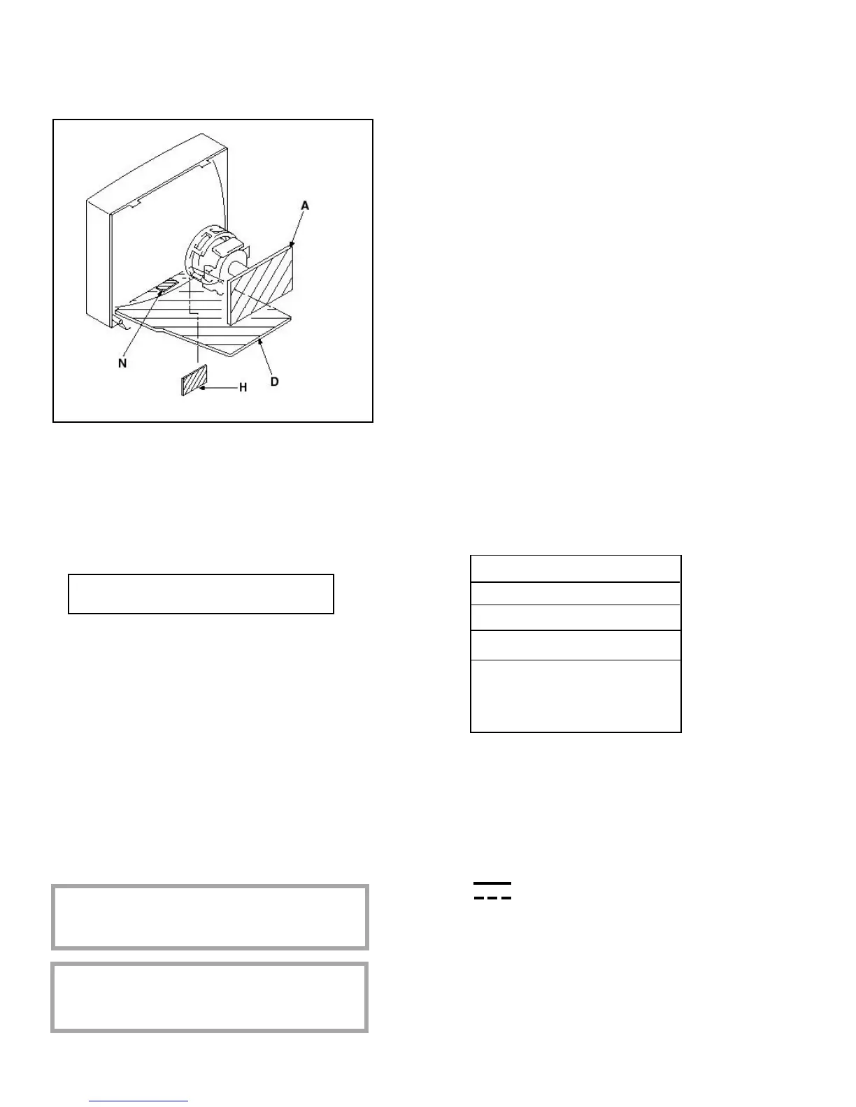
5-2. CIRCUIT BOARDS LOCATION
Note:
•
All capacitors are in µF unless otherwise noted. pF: µµF
50 WV or less are not indicated except for electrolytic.
•
Indication of resistance, which does not have one for rating
electrical power, is as follows.
•
All resistors are in ohms.
• f : nonflammable resistor.
• F : fusible resistor.
• ∆ : internal component.
• p : panel designation and adjustment for repair.
• e : earth-ground.
• E : earth-chassis.
• The components identified by [ in this basic schematic
diagram have been carefully factory-selected for each set
in order to satisfy regulations regarding X-ray radiation.
Should replacement be required, replace only with the
value originally used.
•
When replacing components identified by ], make the necessary
adjustments by using RV904 ([) as indicated. (See page 13)
• All variable and adjustable resistors have characteristic curve B,
unless otherwise noted.
• When replacing parts shown in the table below,
be sure to perform the safety related adjustment.
Part Replaced ([)
RV904
Part Replaced (])
• All voltages are in volts.
• Readings are taken with a 10 ΜΩ digital multimeter
• Readings are taken with a color-bar signal input.
• Voltage variations may be noted due to normal
production tolerances.
• * : Cannot be measured.
• Circled numbers are waveform references.
• : B +bus.
• : B - bus.
Pitch: 5 mm
Rating electrical power 1/4 W (CHIP: 1/10 W)
Note: The components identified by shading and
mark ¡
are critical for safety. Replace only
with part number specified.
Note: Les composants identifies per un trame et une
marque ¡ sont critiques pour la securite. Ne les
remplacer que par une piece portant le numero specifie.
5-3. SCHEMATIC DIAGRAMS AND PRINTED WIRING BOARDS
D - BOARD
T901, R903, IC805, R921, R922,
R812, D908, IC605, R913, R914,
D802, D909
D1