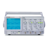
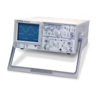
Do you have a question about the GW Instek GOS-6030 and is the answer not in the manual?
Details the reverse engineering process and the document's origin.
Diagram illustrating interconnections between various PCBs in the GOS-6030.
Lists the CPU Board assembly (OS-10P04C-2).
Lists the Input Amp Board assembly (OS-10P01C).
Lists the CRT Board assembly (OS-01P03G-4).
Lists the HV PSU Board assembly (OS-10P03G-1).
Lists the HV PSU Board (Build 2) assembly (OS-10P03F-1).
Lists the LV PSU Board assembly (OS-10P03G-5).
Lists the X Drive Board assembly (OS-10P02D).
Lists the Y Drive Board assembly (OS-10P03G-6).
Lists the Front Panel Board assembly (?).
Lists the Potentiometer Board assembly (OS10P03G-03).
Discusses model variations, PCB commonality across the range, and design differences.
Details the mixture of build styles and the complexity of the X drive board's design.
Warns about sharp edges and provides guidance for accessing internal components.
Highlights common faults like PSU problems, dry joints, and mains switch failures.
Notes difficulties with S/M component identification on the X I/P board.
Schematic of the Low Voltage Power Supply board (P/N OS10P03G-1).
Schematic of the High Voltage Power Supply board (P/N OS10P03G-1).
Details pin functions, voltages for the 150BTB31A CRT tube, and electrical data.
Schematic of the Potentiometer board (OS-10P03G-03).
Schematic detailing the X drive board circuitry (P/N OS10P02D).
Details optional components, connectors, and IC power on the X drive board.
Schematic focusing on gain stages within the X drive board.
Schematic detailing the Y drive board circuitry (OS10P13G-6).
Image of the X Pre Amp Board (OS10P01C) and its components.
Image of the CPU Board (OS10P04C-2) and its components.
| Type | Oscilloscope |
|---|---|
| Bandwidth | 30 MHz |
| Channels | 2 |
| Vertical Sensitivity | 5 mV/div to 5 V/div |
| Rise Time | ≤ 12 ns |
| Trigger Sources | CH1, CH2, Line, Ext |
| Display | CRT |
| Trigger Modes | Auto, Normal, Single |
| Sweep Time | 0.2 μs to 0.5 s/div |
| Input Impedance | 1 MΩ |
| Power Supply | 100-240 VAC, 50/60 Hz |
| Weight | 7.5 kg |
| Sample Rate | 100 MSa/s |
| Input Voltage Range | 400 V (DC + AC peak) |
| Time Base | 0.2 μs/div to 0.5 s/div |


