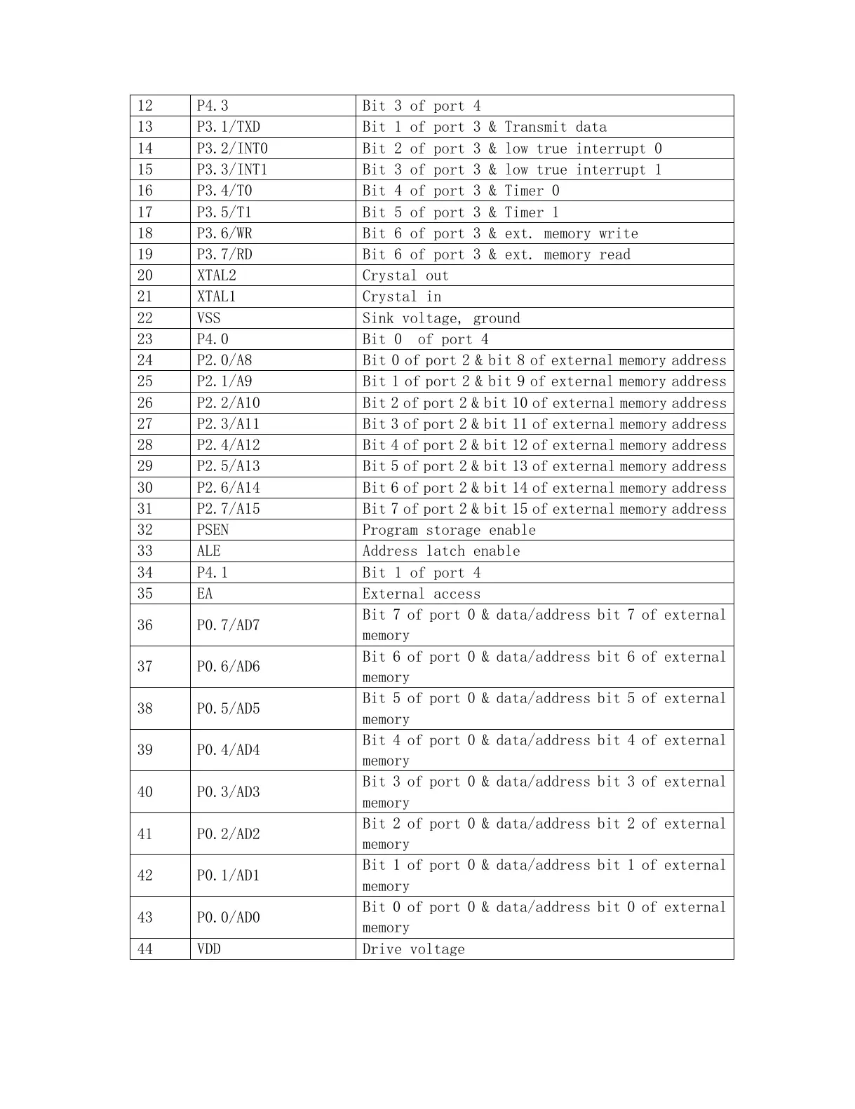
12 P4.3 Bit 3 of port 4
13 P3.1/TXD Bit 1 of port 3 & Transmit data
14 P3.2/INT0 Bit 2 of port 3 & low true interrupt 0
15 P3.3/INT1 Bit 3 of port 3 & low true interrupt 1
16 P3.4/T0 Bit 4 of port 3 & Timer 0
17 P3.5/T1 Bit 5 of port 3 & Timer 1
18 P3.6/WR Bit 6 of port 3 & ext. memory write
19 P3.7/RD Bit 6 of port 3 & ext. memory read
20 XTAL2 Crystal out
21 XTAL1 Crystal in
22 VSS Sink voltage, ground
23 P4.0 Bit 0 of port 4
24 P2.0/A8 Bit 0 of port 2 & bit 8 of external memory address
25 P2.1/A9 Bit 1 of port 2 & bit 9 of external memory address
26 P2.2/A10 Bit 2 of port 2 & bit 10 of external memory address
27 P2.3/A11 Bit 3 of port 2 & bit 11 of external memory address
28 P2.4/A12 Bit 4 of port 2 & bit 12 of external memory address
29 P2.5/A13 Bit 5 of port 2 & bit 13 of external memory address
30 P2.6/A14 Bit 6 of port 2 & bit 14 of external memory address
31 P2.7/A15 Bit 7 of port 2 & bit 15 of external memory address
32 PSEN Program storage enable
33 ALE Address latch enable
34 P4.1 Bit 1 of port 4
35 EA External access
36 P0.7/AD7
Bit 7 of port 0 & data/address bit 7 of external
memory
37 P0.6/AD6
Bit 6 of port 0 & data/address bit 6 of external
memory
38 P0.5/AD5
Bit 5 of port 0 & data/address bit 5 of external
memory
39 P0.4/AD4
Bit 4 of port 0 & data/address bit 4 of external
memory
40 P0.3/AD3
Bit 3 of port 0 & data/address bit 3 of external
memory
41 P0.2/AD2
Bit 2 of port 0 & data/address bit 2 of external
memory
42 P0.1/AD1
Bit 1 of port 0 & data/address bit 1 of external
memory
43 P0.0/AD0
Bit 0 of port 0 & data/address bit 0 of external
memory
44 VDD Drive voltage