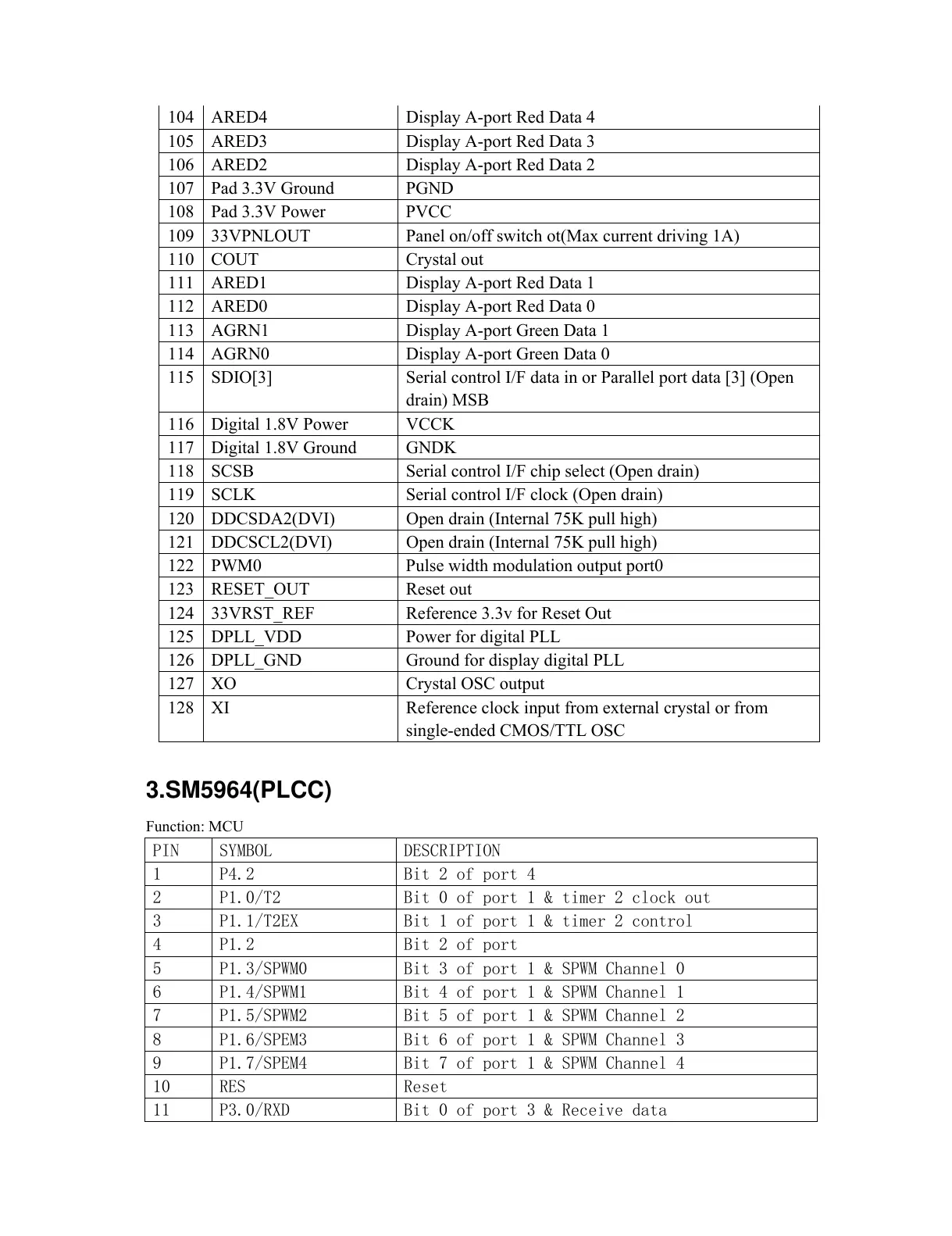
104 ARED4 Display A-port Red Data 4
105 ARED3 Display A-port Red Data 3
106 ARED2 Display A-port Red Data 2
107 Pad 3.3V Ground PGND
108 Pad 3.3V Power PVCC
109 33VPNLOUT Panel on/off switch ot(Max current driving 1A)
110 COUT Crystal out
111 ARED1 Display A-port Red Data 1
112 ARED0 Display A-port Red Data 0
113 AGRN1 Display A-port Green Data 1
114 AGRN0 Display A-port Green Data 0
115 SDIO[3] Serial control I/F data in or Parallel port data [3] (Open
drain) MSB
116 Digital 1.8V Power VCCK
117 Digital 1.8V Ground GNDK
118 SCSB Serial control I/F chip select (Open drain)
119 SCLK Serial control I/F clock (Open drain)
120 DDCSDA2(DVI) Open drain (Internal 75K pull high)
121 DDCSCL2(DVI) Open drain (Internal 75K pull high)
122 PWM0 Pulse width modulation output port0
123 RESET_OUT Reset out
124 33VRST_REF Reference 3.3v for Reset Out
125 DPLL_VDD Power for digital PLL
126 DPLL_GND Ground for display digital PLL
127 XO Crystal OSC output
128 XI Reference clock input from external crystal or from
single-ended CMOS/TTL OSC
3.SM5964(PLCC)
Function: MCU
PIN SYMBOL DESCRIPTION
1 P4.2 Bit 2 of port 4
2 P1.0/T2 Bit 0 of port 1 & timer 2 clock out
3 P1.1/T2EX Bit 1 of port 1 & timer 2 control
4 P1.2 Bit 2 of port
5 P1.3/SPWM0 Bit 3 of port 1 & SPWM Channel 0
6 P1.4/SPWM1 Bit 4 of port 1 & SPWM Channel 1
7 P1.5/SPWM2 Bit 5 of port 1 & SPWM Channel 2
8 P1.6/SPEM3 Bit 6 of port 1 & SPWM Channel 3
9 P1.7/SPEM4 Bit 7 of port 1 & SPWM Channel 4
10 RES Reset
11 P3.0/RXD Bit 0 of port 3 & Receive data